A29DL323 Series
32M-Bit CMOS Low Voltage Dual Operation Flash Memory
Preliminary
4M-Byte by 8-Bit (Byte Mode) / 2M-Word by 16-Bit (Word Mode)
PRELIMINARY (May, 2002, Version 0.0)
1
AMIC Technology, Inc.
Features
n
Two bank organization enabling simultaneous execution of
erase / program and read
n
Bank organization: 2 banks (8 Mbits + 24 Mbits)
n
Memory organization:
- 4,194,304 words x
8 bits (BYTE mode)
- 2,097,152 words x
16 bits (WORD mode)
n
Sector organization:
71 sectors (8 Kbytes / 4 Kwords ◊ 8 sectors, 64 Kbytes /
32 Kwords ◊ 63 sectors)
n
2 types of sector organization
- T type: Boot sector allocated to the highest address
(sector)
- B type: Boot sector allocated to the lowest address
(sector)
n
3-state output
n
Automatic program
- Program suspend / resume
n
Unlock bypass program
n
Automatic erase
- Chip erase
- Sector erase (sectors can be combined freely)
n
Erase suspend / resume
n
Program / Erase completion detection
- Detection through data polling and toggle bits
- Detection through RY/
BY
pin
n
Sector group protection
- Any sector group can be protected
- Any protected sector group can be temporary
unprotected
n
Sectors can be used for boot application
n
Hardware reset and standby using
RESET
pin
n
Automatic sleep mode
n
Boot block sector protect by
WP
(ACC) pin
n
Conforms to common flash memory interface (CFI)
n
Extra One Time Protect Sector provided
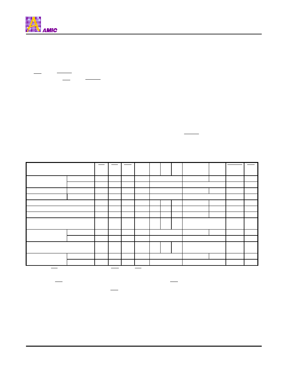
Part No.
Access
time
(Max.)
Operating
supply
voltage
Power supply current
(Active mode)
(Max.)
Standby
current
(Max.)
A29DL323 90ns
2.7V~
3.6V
16mA
30mA
5 A
n
Operating ambient temperature: -40 to 85∞C
n
Program / erase time
- Program: 9.0 µs / byte (TYP.)
11.0 µs / word (TYP.)
- Sector erase: 0.7 s (TYP.)
n
Number of program / erase: 1,000,000 times (MIN.)
n
Package options
-
48-pin TSOP (I) or 63-ball TFBGA
General Description
The A29DL323 is a flash memory organized of 33,554,432
bits and 71 sectors. Sectors of this memory can be erased
at a low voltage (2.7 to 3.6 V) supplied from a single power
source, or the contents of the entire chip can be erased.
Two modes of memory organization, BYTE mode
(4,194,304 words ◊ 8 bits) and WORD mode (2,097,152
words ◊ 16 bits), are selectable so that the memory can be
programmed in byte or word units.
The A29DL323 can be read while its contents are being
erased or programmed. The memory cell is divided into two
banks. While sectors in one bank are being erased or
programmed, data can be read from the other bank thanks
to the simultaneous execution architecture. The banks are
8 Mbits and 24 Mbits.
This flash memory comes in two types. The T type has a
boot sector located at the highest address (sector) and the
B type has a boot sector at the lowest address (sector).
Because the A29DL323 enables the boot sector to be
erased, it is ideal for storing a boot program. In addition,
program code that controls the flash memory can be also
stored, and the program code can be programmed or
erased without the need to load it into RAM. Eight small
sectors for storing parameters are provided, each of which
can be erased in 8 Kbytes units.
Once a program or erase command sequence has been
executed, an automatic program or automatic erase
function internally executes program or erase and
verification automatically.
Because the A29DL323 can be electrically erased or
programmed by writing an instruction, data can be
reprogrammed on-board after the flash memory has been
installed in a system, making it suitable for a wide range of
applications.
A29DL323 Series
PRELIMINARY (May, 2002, Version 0.0)
2
AMIC Technology, Inc.
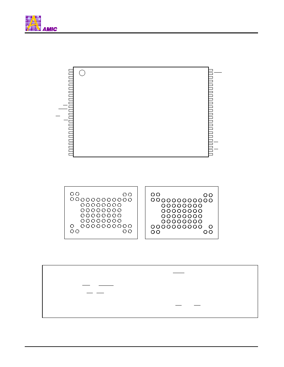
Pin Configurations
n
TSOP (I)
A29DL323V
1
2
3
4
5
6
7
8
9
10
11
12
13
14
15
16
A14
A13
A12
A11
A10
A9
A8
A20
WE
RESET
NC
WP (ACC)
RY/BY
A18
48
47
46
45
44
43
42
41
40
39
38
37
36
35
34
33
I/O
2
I/O
10
I/O
3
I/O
11
VCC
I/O
4
I/O
12
I/O
5
I/O
13
I/O
6
I/O
14
I/O
7
I/O
15
(A-1)
GND
BYTE
A16
A15
A19
17
18
19
20
21
22
23
24
25
26
27
28
29
30
31
32
I/O
9
I/O
1
I/O
8
I/O
0
OE
GND
CE
A0
A17
A7
A6
A5
A4
A3
A2
A1
n
TFBGA
Top View
Bottom View
8
7
6
5
4
3
2
1
A B C D E F G H J K L M
A
B
C
D
E
F
G
H
J
K
L
M
Top View
A
B
C
D
E
F
G
H
J
K
L
M
1
NC
NC
NC
NC
2
NC
NC
A13
A12
A14
A15
A16
BYTE
I/O
15
(A-1) GND
NC
NC
3
A9
A8
A10
A11
I/O
7
I/O
14
I/O
13
I/O
6
4
WE
RESET
NC
A19
I/O
5
I/O
12
VCC
I/O
4
5
RY/
BY
WP
(ACC) A18
A20
I/O
2
I/O
10
I/O
11
I/O
3
6
A7
A17
A6
A5
I/O
0
I/O
8
I/O
9
I/O
1
7
NC
A3
A4
A2
A1
A0
CE
OE
GND
NC
NC
8
NC
NC
NC
NC
A29DL323 Series
PRELIMINARY (May, 2002, Version 0.0)
3
AMIC Technology, Inc.
Block Diagram
Address
Buffers
Bank / Sector
Decoder
State
Control
(Command
Register)
Address Latch
Address Latch
X-Decoder
Y-Decoder
Cell Matrix
(Bank 1)
Y-Gating
X-Decoder
Y-Decoder
Cell Matrix
(Bank 2)
Y-Gating
SA / WC
Data Latch
SA / WC
Input / Output
Buffers
I/O
0
- I/O
15
(A-1)
WP(ACC)
A0-A20
VCC
GND
RY/BY
Bank 1 Address
RESET
WE
BYTE
CE
OE
Bank 2 Address
Program / Erase
Voltage Generator
Pin Descriptions
Pin No.
Description
A0 ≠ A20
Address Inputs
I/O
0
- I/O
14
Data Inputs/Outputs
I/O
15
Data Input/Output, Word Mode
I/O
15
(A-1)
A-1
LSB Address Input, Byte Mode
CE
Chip Enable
WE
Write Enable
OE
Output Enable
RESET
Hardware Reset Input
BYTE
Mode Select
RY/
BY
Ready/
BUSY
- Output
WP
(ACC)
Write Protect (Accelerated) Input
GND
Ground
VCC
Power Supply
NC
Note
No Connection
Note:
Some signals can be applied because this pin is not connected to the inside of the chip.
A29DL323 Series
PRELIMINARY (May, 2002, Version 0.0)
4
AMIC Technology, Inc.
Input / Output Pin Function
Pin Name
Input / Output
Function
A0 to A20
Input
Address input pins.
A0 to A20 are used differently in the BYTE mode and the WORD mode.
BYTE MODE
A0 to A20 are used as the upper 21 bits of total 22 bits of address input pin.
(The least significant bit (A-1) is combined to I/O
15
.)
WORD MODE
A0 to A20 are used as 21 bits address input pin.
I/O
0
to I/O
14
Input / Output
Data input / output pins.
I/O
0
to I/O
14
are used differently in the BYTE mode and the WORD mode.
BYTE MODE
I/O
0
to I/O
7
are used as the 8 bits data input / output pins.
I/O
8
to I/O
14
are Hi-Z.
WORD MODE
I/O
0
to I/O
14
are used as the lower 15 bits of total 16 bits of data input / output pins.
(The most significant bit (I/O15) is combined to A-1.)
I/O
15
, A-1
Input / Output
I/O
15
, A1 are used differently in the BYTE mode and the WORD mode.
BYTE MODE
The least significant address input pin (A-1)
WORD MODE
The most significant data input / output pin (I/O
15
)
CE
Input
This pin inputs the signal that activates the chip.
When high level, the chip enters the standby mode.
OE
Input
This pin inputs the read operation control signal.
When high level, output is Hi-Z.
WE
Input
This pin inputs the write operation control signal.
When low level, command input is accepted.
BYTE
Input
The pin for switching BYTE mode and WORD mode.
High level : WORD MODE (2M words x 16 bits)
Low level : BYTE MODE (4M words x 8 bits)
RESET
Input
This pin inputs hardware reset.
When low level, hardware reset is performed.
If 11.5 to 12.5 V is applied to
RESET
, the chip enters the temporary sector group
unprotect mode.
RY
/BY
Output
This pin indicates whether automatic program / erase is currently being executed. It uses
open drain connection.
Low level indicates the busy state during which the device is performing automatic
program erase.
High level indicates the device is in the ready state and will accept the next operation. In
this case, the device is either in the erase suspend mode or the standby mode.
WP (ACC)
Input
This pin selects the boot block sector protect mode or accelerated mode.
Low level: The boot block (2 sectors) is protected.
High level: The boot block is unprotected.
VACC level: Accelerated mode is selected.
VCC
-
Supply Voltage
GND
-
Ground
NC
-
No Connection
A29DL323 Series
PRELIMINARY (May, 2002, Version 0.0)
5
AMIC Technology, Inc.
Absolute Maximum Ratings*
Storage Temperature (T
stg
) . . . . . . . . . . -55
∞
C to + 125
∞
C
Operating Ambient Temperature (T
A
) . . . . . . . . . . . . . . . . . .
. . . . . . . . . . . . . . . . . . . . . . . . . . . . . . . . . . -40
∞
C to + 85
∞
C
Input / Output Voltage with Respect to GND
WP
(ACC),
RESET
. . . . . . . . . . . . -0.5V
Note1
to 13.0V
All Pins except
WP
(ACC),
RESET
. . . . . . . . . . . . . . .
. . . . . . . . . . . . . -0.5V
Note1
to VCC + 0.4 (4.0V max.)
Note2
Supply Voltage with Respect to GND (VCC)
. . . . . . . . . . . . . . . . . . . . . . . . . . . . . . . . . . . . . -0.5V to 4.0V
Notes:
1. -2.0V (Min.) (Pulse width
20ns)
2. VCC + 0.5V (Max.) (Pulse width
20ns)
*Comments
Stresses above those listed under "Absolute Maximum
Ratings" may cause permanent damage to this device.
These are stress ratings only. Functional operation of
this device at these or any other conditions above
those indicated in the operational sections of these
specification is not implied or intended. Exposure to
the absolute maximum rating conditions for extended
periods may affect device reliability.
Recommended Operating Conditions
Operating Ambient Temperature (T
A
) . . . . . . . . . . . . . . . . . .
. . . . . . . . . . . . . . . . . . . . . . . . . . . . . . . . . . . -40
∞
C to +85
∞
C
Supply Voltage (VCC) . . . . . . . . . . . . . . . . . +2.7V to +3.6V
Bus Operations
The following table shows the operation modes of the dual
operation flash memory. Before turning on power, input
GND
±
0.2 V to the
RESET
until VCC
VCC (min.).
Table 1. A29DL323 Bus Operations
Operation
CE
OE
WE
I/O
15
,
A-1
A6 A1 A0
I/O
0
to
I/O
7
I/O
8
to
I/O
15
RESET
WP
(ACC)
BYTE mode
L
L
H
A-1
Address input
Data output
Hi-Z
H
X
Read (Note)
WORD mode
L
L
H
X
Address input
Data output
H
X
Write
BYTE mode
L
H
L
A-1
Address input
Data input
Hi-Z
H
Note3
WORD mode
L
H
L
X
Address input
Data input
H
Note3
Standby
H
X
X
X
X
X
X
Hi-Z
Hi-Z
H
X
Hardware reset / Standby
X
X
X
X
X
X
X
Hi-Z
Hi-Z
L
X
Output Disable
L
H
H
X
X
X
X
Hi-Z
Hi-Z
H
X
Temporary Sector Group Unprotect
X
X
X
X
X
X
X
Hi-Z or
Data input / output
V
ID
Note3
BYTE mode
L
L
H
A-1
Address input
Data output
Hi-Z
H
X
Automatic Sleep
Mode
WORD mode
L
L
H
X
Address input
Data output
H
X
Boot Block Sector Protect
X
X
X
X
X
X
X
Hi-Z or
Data input / output
X
L
BYTE mode
L
H
L
A-1
Address input
Data input
Hi-Z
H
VACC
Accelerated Mode
WORD mode
L
H
L
X
Address input
Data input
H
VACC
Note: When
OE
= V
IL
, V
IL
can be applied to
WE
. When
OE
= V
IH
, a write operation is started.
Remarks: 1. H : V
IH
, L : V
IL
, : V
IH
or V
IL
, V
ID
: 11.5 V to 12.5 V, VACC : 8.5 V to 9.5 V
2. If an address is held longer than the minimum read cycle time (t
RC
), the automatic sleep mode is set.
3. If
WP
(ACC)=V
IL
, sector 0,1,140, and 141 remain protected. If
WP
(ACC)=V
IH
,
protection on sectors 0,1,140, and 141
depends on whether they were last protected or unprotected using the method described in "Sector/Sector Block
Protection and Unprotection". If
WP
(ACC)=V
HH
, all sectors will be unprotected.

A29DL323 Series
PRELIMINARY (May, 2002, Version 0.0)
6
AMIC Technology, Inc.
Read Operation
The read operation is controlled by the
OE
and /OE. The
/CE is used to select a device, and the
OE
controls data
output. The following three access times are used
depending on the condition.
-
Address access time (t
ACC
): Time until valid data is
output after an address has been determined
(however, after
CE
).
-
CE
access time (t
CE)
: Time until valid data is output
after
CE
has been determined (however, after
address).
-
OE
access time (t
OE
): Time until valid data is output
after
OE
has been determined (however,
OE
must
be input after t
ACC
-t
OE
, t
CE
-t
OE
after address and
CE
have been determined).
On power-up, the device is automatically set in the read
mode. To read the device without changing address
immediately after power application, either execute
hardware reset or briefly lower
CE
to V
IL
from V
IH
.
For the timing waveform, refer to Timing Waveform for
Read Cycle (1).
Write Operation
The operation of the device is controlled by writing
commands to the registers. The command register is a
function that latches the address and data necessary for
executing an instruction and does not occupy the memory
area.
If an illegal address or data is written or if an address or
data is written in the wrong sequence, the device is reset to
the read mode.
Standby Mode
The standby mode is set when V
IH
is input to the
CE
. The
current consumption in the standby mode can be lowered to
5
µ
A or less in two ways.
One is to use
CE
and RESET. Input VCC
±
0.3 V to
CE
and RESET . However, while automatic programming or
erasing is being executed, the operating supply current
(I
CC2
) does not decrease to 5
µ
A or lower even if
CE
= V
IH
.
If a read operation is executed in the standby mode, data is
output at
CE
access time.
The other is to input GND
±
0.3 V to the RESET. At this
time, the level of
CE
is V
IH
or V
IL
. In this case, t
RH
is
required for the device to return to the read mode from the
standby mode.
For the timing waveform, refer to Timing Waveform for
Read Cycle (2).
Hardware Reset Pin
The device is reset to the read mode if V
IL
is input to the
RESET for the duration of t
RP
and V
IH
for the duration of
t
RH
. While V
IL
is being input to the RESET, all commands
are ignored, and the output pins go into a Hi-Z state. If the
voltage on RESET is kept to GND
±
0.2 V at this time, the
current consumption can be lowered to 5
µ
A or less. If V
IH
is
input to the RESET, t
READY
is required until data is output.
For the timing waveform, refer to Timing Waveform for
Read Cycle (2).
Output Disable Mode
Output from the device is disabled (Hi-Z state) if V
IH
is input
to the
OE
.
Sector Group Protection
Protect the sector group by using a command.
OE
or
WE
control is no need.
Temporary Sector Group Unprotect
Protection of a sector group can be temporarily canceled.
When V
ID
is input to RESET, the temporary sector group
unprotect mode is set. If a protected sector is selected in
this mode, it can be programmed or erased. If the mode is
canceled, the sector group is protected again.
For the timing waveform, refer to Timing Waveform for
Temporary Sector Group Unprotect.
Product ID
Read the product ID code by using a command.
Automatic Sleep Mode
The automatic sleep mode is used to reduce the power
consumption substantially during a read operation.
If an address is held longer than the minimum read
cycle time (t
RC
), the sleep mode (low power
consumption
mode) is automatically set. In this mode, the
output data is latched and continuously output.
In the automatic sleep mode,
CE
,
WE
, and
OE
do not
have to be controlled. At this time, the current consumption
decreases to 5
µ
A or less. During dual operation,
however, the current consumption is power supply
current (I
CC6
, I
CC7
).
If the address is changed, the automatic sleep mode
is canceled automatically, the device returns to the
read mode, and the data of the newly input address is
output.
A29DL323 Series
PRELIMINARY (May, 2002, Version 0.0)
7
AMIC Technology, Inc.
Boot Block Sector Protect
The boot block sector protect mode protects the two sectors
of the boot block. This mode is set when V
IL
is input to
WP
(ACC). If V
IL
is input to
WP
(ACC) even in the temporary
sector group unprotect mode, the boot block remains
protected and protection of the other sectors is temporarily
canceled.
Accelerated Mode
This mode is used to program the device at high speed,
and the programming time can be shortened to about 60%.
To program the device in the accelerated mode, input
VACC to
WP
(ACC) and use an unlock bypass program
command. Therefore, ordinary commands can be used for
programming or detection of completion of programming.
If VACC is input to
WP
(ACC), the device is automatically
set in the unlock bypass mode. Therefore, the unlock
bypass set command and reset command are not
necessary. The accelerated mode is automatically canceled
if the input of VACC to
WP
(ACC) is stopped.
In the accelerated mode, protection of the sector group is
temporarily canceled. Exercise care in programming the
device at this time.
For the timing waveform, refer to Timing Waveform for
Accelerated Mode.
Dual Operation
This device can execute a program or erase operation and
a read operation simultaneously. By selecting bank 1 or 2
by changing the bank address, one bank can execute a
read operation while the other bank is executing a program
or erase operation. When changing the bank address, no
wait cycle is necessary. Note that two or more program or
erase operation. When changing the bank address, no wait
cycle is necessary. Note that two or more operations cannot
be executed at the same time in the same bank.
The following table shows the combinations of bank
operations.
For the timing waveform, refer to Timing Waveform for Dual
Operation.
Table 2. Dual Operation
Case
Operation of Bank 1
Operation of Bank 2
1
Read mode
Read mode
2
Read mode
Product ID
3
Read mode
Program (Note 1)
4
Read mode
Erase (Note 2)
5
Product ID
Read mode
6
Program (Note 1)
Read mode
7
Erase (Note 2)
Read mode
Notes 1. The program operation is suspended by the program suspend command, and addresses not
being programmed to at this time can only be read.
2. The erase operation is suspended by the erase suspend command. The sector not erased at
this time can be read or programmed.
A29DL323 Series
PRELIMINARY (May, 2002, Version 0.0)
8
AMIC Technology, Inc.
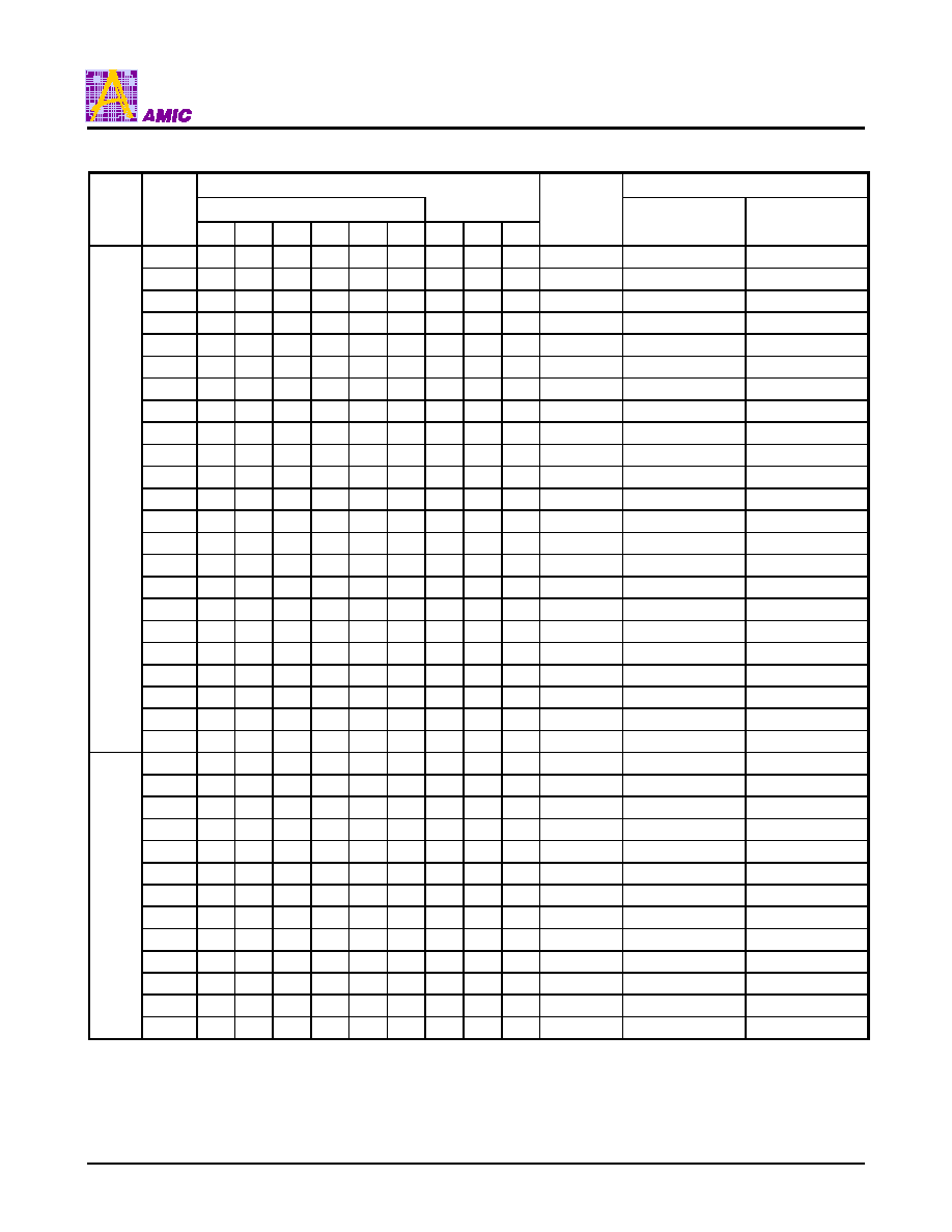
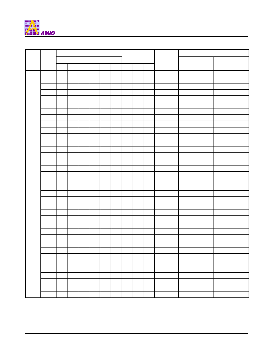
Table 3. A29DL323 Top Boot Block Sector Address Table
Sector Address Table
Address Range (in hexadecimal)
Bank Address Table
Bank Sector
A20 A19 A18 A17 A16 A15 A14 A13 A12
Sector Size
(Kbytes/
Kwords)
Byte Mode
(x 8)
Word Mode
(x16)
SA70
1
1
1
1
1
1
1
1
1
8/4
3FFFFFH-3FE000H 1FFFFFH-1FF000H
SA69
1
1
1
1
1
1
1
1
0
8/4
3FDFFFH-3FC000H 1FEFFFH-1FE000H
SA68
1
1
1
1
1
1
1
0
1
8/4
3FBFFFH-3FA000H 1FDFFFH-1FD000H
SA67
1
1
1
1
1
1
1
0
0
8/4
3F9FFFH-3F8000H 1FCFFFH-1FC000H
SA66
1
1
1
1
1
1
0
1
1
8/4
3F7FFFH-3F6000H 1FBFFFH-1FB000H
SA65
1
1
1
1
1
1
0
1
0
8/4
3F5FFFH-3F4000H 1FAFFFH-1FA000H
SA64
1
1
1
1
1
1
0
0
1
8/4
3F3FFFH-3F2000H 1F9FFFH-1F9000H
SA63
1
1
1
1
1
1
0
0
0
8/4
3F1FFFH-3F0000H 1F8FFFH-1F8000H
SA62
1
1
1
1
1
0
X
X
X
64/32
3EFFFFH-3E0000H 1F7FFFH-1F0000H
SA61
1
1
1
1
0
1
X
X
X
64/32
3DFFFFH-3D0000H 1EFFFFH-1E8000H
SA60
1
1
1
1
0
0
X
X
X
64/32
3CFFFFH-3C0000H 1E7FFFH-1E0000H
SA59
1
1
1
0
1
1
X
X
X
64/32
3BFFFFH-3B0000H 1DFFFFH-1D8000H
SA58
1
1
1
0
1
0
X
X
X
64/32
3AFFFFH-3A0000H 1D7FFFH-1D0000H
SA57
1
1
1
0
0
1
X
X
X
64/32
39FFFFH-390000H 1CFFFFH-1C8000H
SA56
1
1
1
0
0
0
X
X
X
64/32
38FFFFH-380000H 1C7FFFH-1C0000H
SA55
1
1
0
1
1
1
X
X
X
64/32
37FFFFH-370000H 1BFFFFH-1B8000H
SA54
1
1
0
1
1
0
X
X
X
64/32
36FFFFH-360000H 1B7FFFH-1B0000H
SA53
1
1
0
1
0
1
X
X
X
64/32
35FFFFH-350000H 1AFFFFH-1A8000H
SA52
1
1
0
1
0
0
X
X
X
64/32
34FFFFH-340000H 1A7FFFH-1A0000H
SA51
1
1
0
0
1
1
X
X
X
64/32
33FFFFH-330000H 19FFFFH-198000H
SA50
1
1
0
0
1
0
X
X
X
64/32
32FFFFH-320000H 197FFFH-190000H
SA49
1
1
0
0
0
1
X
X
X
64/32
31FFFFH-310000H 18FFFFH-188000H
Bank 1
SA48
1
1
0
0
0
0
X
X
X
64/32
30FFFFH-300000H 187FFFH-180000H
SA47
1
0
1
1
1
1
X
X
X
64/32
2FFFFFH-2F0000H 17FFFFH-178000H
SA46
1
0
1
1
1
0
X
X
X
64/32
2EFFFFH-2E0000H 177FFFH-170000H
SA45
1
0
1
1
0
1
X
X
X
64/32
2DFFFFH-2D0000H 16FFFFH-168000H
SA44
1
0
1
1
0
0
X
X
X
64/32
2CFFFFH-2C0000H 167FFFH-160000H
SA43
1
0
1
0
1
1
X
X
X
64/32
2BFFFFH-2B0000H 15FFFFH-158000H
SA42
1
0
1
0
1
0
X
X
X
64/32
2AFFFFH-2A0000H 157FFFH-150000H
SA41
1
0
1
0
0
1
X
X
X
64/32
29FFFFH-290000H 14FFFFH-148000H
SA40
1
0
1
0
0
0
X
X
X
64/32
28FFFFH-280000H 147FFFH-140000H
SA39
1
0
0
1
1
1
X
X
X
64/32
27FFFFH-270000H 13FFFFH-138000H
SA38
1
0
0
1
1
0
X
X
X
64/32
26FFFFH-260000H 137FFFH-130000H
SA37
1
0
0
1
0
1
X
X
X
64/32
25FFFFH-250000H 12FFFFH-128000H
SA36
1
0
0
1
0
0
X
X
X
64/32
24FFFFH-240000H 127FFFH-120000H
Bank 2
SA35
1
0
0
0
1
1
X
X
X
64/32
23FFFFH-230000H 11FFFFH-118000H
A29DL323 Series
PRELIMINARY (May, 2002, Version 0.0)
9
AMIC Technology, Inc.
Table 3. A29DL323 Top Boot Block Sector Address Table (continued)
Sector Address Table
Address Range (in hexadecimal)
Bank Address Table
Bank Sector
A20 A19 A18 A17 A16 A15 A14 A13 A12
Sector Size
(Kbytes/
Kwords)
Byte Mode
(x 8)
Word Mode
(x16)
SA34
1
0
0
0
1
0
X
X
X
64/32
22FFFFH-220000H 117FFFH-110000H
SA33
1
0
0
0
1
1
X
X
X
64/32
21FFFFH-210000H 10FFFFH-108000H
SA32
1
0
0
0
0
0
X
X
X
64/32
20FFFFH-200000H 107FFFH-100000H
SA31
0
1
1
1
1
1
X
X
X
64/32
1FFFFFH-1F0000H 0FFFFFH-0F8000H
SA30
0
1
1
1
1
0
X
X
X
64/32
1EFFFFH-1E0000H 0F7FFFH-0F0000H
SA29
0
1
1
1
0
1
X
X
X
64/32
1DFFFFH-1D0000H 0EFFFFH-0E8000H
SA28
0
1
1
1
0
0
X
X
X
64/32
1CFFFFH-1C0000H 0E7FFFH-0E0000H
SA27
0
1
1
0
1
1
X
X
X
64/32
1BFFFFH-1B0000H 0DFFFFH-0D8000H
SA26
0
1
1
0
1
0
X
X
X
64/32
1AFFFFH-1A0000H 0D7FFFH-0D0000H
SA25
0
1
1
0
0
1
X
X
X
64/32
19FFFFH-190000H 0CFFFFH-0C8000H
SA24
0
1
1
0
0
0
X
X
X
64/32
18FFFFH-180000H 0C7FFFH-0C0000H
SA23
0
1
0
1
1
1
X
X
X
64/32
17FFFFH-170000H 0BFFFFH-0B8000H
SA22
0
1
0
1
1
0
X
X
X
64/32
16FFFFH-160000H 0B7FFFH-0B0000H
SA21
0
1
0
1
0
1
X
X
X
64/32
15FFFFH-150000H 0AFFFFH-0A8000H
SA20
0
1
0
1
0
0
X
X
X
64/32
14FFFFH-140000H 0A7FFFH-0A0000H
SA19
0
1
0
0
1
1
X
X
X
64/32
13FFFFH-130000H 09FFFFH-098000H
SA18
0
1
0
0
1
0
X
X
X
64/32
12FFFFH-120000H 097FFFH-090000H
SA17
0
1
0
0
0
1
X
X
X
64/32
11FFFFH-110000H 08FFFFH-088000H
SA16
0
0
1
0
0
0
X
X
X
64/32
10FFFFH-100000H 087FFFH-080000H
SA15
0
0
1
1
1
1
X
X
X
64/32
0FFFFFH-0F0000H 07FFFFH-078000H
SA14
0
0
1
1
1
0
X
X
X
64/32
0EFFFFH-0E0000H 077FFFH-070000H
SA13
0
0
1
1
0
1
X
X
X
64/32
0DFFFFH-0D0000H 06FFFFH-068000H
SA12
0
0
1
1
0
0
X
X
X
64/32
0CFFFFH-0C0000H 067FFFH-060000H
SA11
0
0
1
0
1
1
X
X
X
64/32
0BFFFFH-0B0000H 05FFFFH-058000H
SA10
0
0
1
0
1
0
X
X
X
64/32
0AFFFFH-0A0000H 057FFFH-050000H
SA9
0
0
1
0
0
1
X
X
X
64/32
09FFFFH-090000H 04FFFFH-048000H
SA8
0
0
1
0
0
0
X
X
X
64/32
08FFFFH-080000H 047FFFH-040000H
SA7
0
0
0
1
1
1
X
X
X
64/32
07FFFFH-070000H 03FFFFH-038000H
SA6
0
0
0
1
1
0
X
X
X
64/32
06FFFFH-060000H 037FFFH-030000H
SA5
0
0
0
1
0
1
X
X
X
64/32
05FFFFH-050000H 02FFFFH-028000H
SA4
0
0
0
1
0
0
X
X
X
64/32
04FFFFH-040000H 027FFFH-020000H
SA3
0
0
0
0
1
1
X
X
X
64/32
03FFFFH-030000H 01FFFFH-018000H
SA2
0
0
0
0
1
0
X
X
X
64/32
02FFFFH-020000H 017FFFH-010000H
SA1
0
0
0
0
0
1
X
X
X
64/32
01FFFFH-010000H 00FFFFH-008000H
Bank 2
SA0
0
0
0
0
0
0
X
X
X
64/32
00FFFFH-000000H 007FFFH-000000H
A29DL323 Series
PRELIMINARY (May, 2002, Version 0.0)
10
AMIC Technology, Inc.
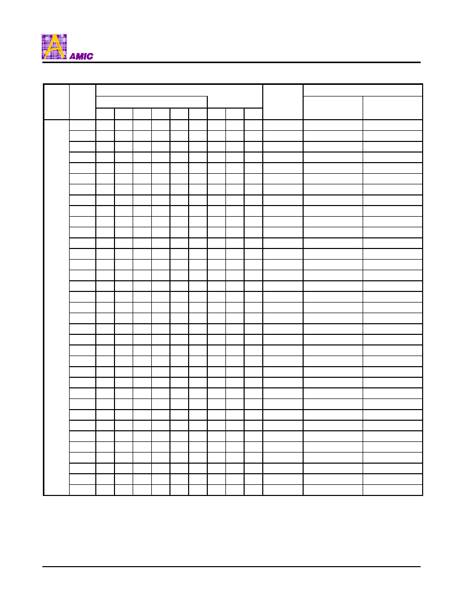
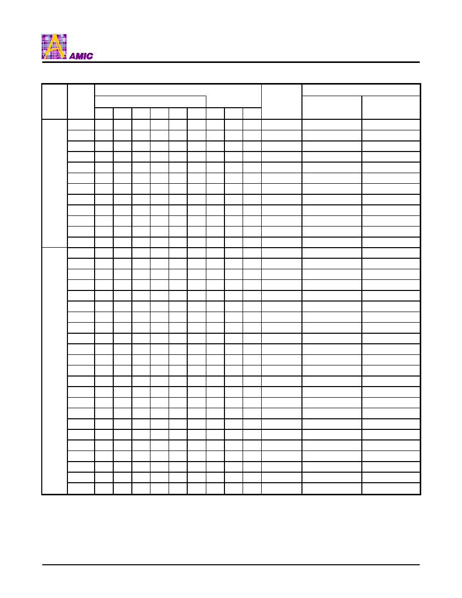
Table 4. A29DL323 Bottom Boot Block Sector Address Table
Sector Address Table
Address Range (in hexadecimal)
Bank Address Table
Bank Sector
A20 A19 A18 A17 A16 A15 A14 A13 A12
Sector Size
(Kbytes/
Kwords)
Byte Mode
(x 8)
Word Mode
(x16)
SA70
1
1
1
1
1
1
X
X
X
64/32
3FFFFFH-3F0000H 1FFFFFH-1F8000H
SA69
1
1
1
1
1
0
X
X
X
64/32
3EFFFFH-3E0000H 1F7FFFH-1F0000H
SA68
1
1
1
1
0
1
X
X
X
64/32
3DFFFFH-3D0000H 1EFFFFH-1E8000H
SA67
1
1
1
1
0
0
X
X
X
64/32
3CFFFFH-3C0000H 1E7FFFH-1E0000H
SA66
1
1
1
0
1
1
X
X
X
64/32
3BFFFFH-3B0000H 1DFFFFH-1D8000H
SA65
1
1
1
0
1
0
X
X
X
64/32
3AFFFFH-3A0000H 1D7FFFH-1D0000H
SA64
1
1
1
0
0
1
X
X
X
64/32
39FFFFH-390000H 1CFFFFH-1C8000H
SA63
1
1
1
0
0
0
X
X
X
64/32
38FFFFH-380000H 1C7FFFH-1C0000H
SA62
1
1
0
1
1
1
X
X
X
64/32
37FFFFH-370000H 1BFFFFH-1B8000H
SA61
1
1
0
1
1
0
X
X
X
64/32
36FFFFH-360000H 1B7FFFH-1B0000H
SA60
1
1
0
1
0
1
X
X
X
64/32
35FFFFH-350000H 1AFFFFH-1A8000H
SA59
1
1
0
1
0
0
X
X
X
64/32
34FFFFH-340000H 1A7FFFH-1A0000H
SA58
1
1
0
0
1
1
X
X
X
64/32
33FFFFH-330000H 19FFFFH-198000H
SA57
1
1
0
0
1
0
X
X
X
64/32
32FFFFH-320000H 197FFFH-190000H
SA56
1
1
0
0
0
1
X
X
X
64/32
31FFFFH-310000H 18FFFFH-188000H
SA55
1
1
0
0
0
0
X
X
X
64/32
30FFFFH-300000H 187FFFH-180000H
SA54
1
0
1
1
1
1
X
X
X
64/32
2FFFFFH-2F0000H 17FFFFH-178000H
SA53
1
0
1
1
1
0
X
X
X
64/32
2EFFFFH-2E0000H 177FFFH-170000H
SA52
1
0
1
1
0
1
X
X
X
64/32
2DFFFFH-2D0000H 16FFFFH-168000H
SA51
1
0
1
1
0
0
X
X
X
64/32
2CFFFFH-2C0000H 167FFFH-160000H
SA50
1
0
1
0
1
1
X
X
X
64/32
2BFFFFH-2B0000H 15FFFFH-158000H
SA49
1
0
1
0
1
0
X
X
X
64/32
2AFFFFH-2A0000H 157FFFH-150000H
SA48
1
0
1
0
0
1
X
X
X
64/32
29FFFFH-290000H 14FFFFH-148000H
SA47
1
0
1
0
0
0
X
X
X
64/32
28FFFFH-280000H 147FFFH-140000H
SA46
1
0
0
1
1
1
X
X
X
64/32
27FFFFH-270000H 13FFFFH-138000H
SA45
1
0
0
1
1
0
X
X
X
64/32
26FFFFH-260000H 137FFFH-130000H
SA44
1
0
0
1
0
1
X
X
X
64/32
25FFFFH-250000H 12FFFFH-128000H
SA43
1
0
0
1
0
0
X
X
X
64/32
24FFFFH-240000H 127FFFH-120000H
SA42
1
0
0
0
1
1
X
X
X
64/32
23FFFFH-230000H 11FFFFH-118000H
SA41
1
0
0
0
1
0
X
X
X
64/32
22FFFFH-220000H 117FFFH-110000H
SA40
1
0
0
0
0
1
X
X
X
64/32
21FFFFH-210000H 10FFFFH-108000H
SA39
1
0
0
0
0
0
X
X
X
64/32
20FFFFH-200000H 107FFFH-100000H
SA38
0
1
1
1
1
1
X
X
X
64/32
1FFFFFH-1F0000H 0FFFFFH-0F8000H
SA37
0
1
1
1
1
0
X
X
X
64/32
1EFFFFH-1E0000H 0F7FFFH-0F0000H
SA36
0
1
1
1
0
1
X
X
X
64/32
1DFFFFH-1D0000H 0EFFFFH-0E8000H
Bank 2
SA35
0
1
1
1
0
0
X
X
X
64/32
1CFFFFH-1C0000H 0E7FFFH-0E0000H
A29DL323 Series
PRELIMINARY (May, 2002, Version 0.0)
11
AMIC Technology, Inc.
Table 4. A29DL323 Bottom Boot Block Sector Address Table (continued)
Sector Address Table
Address Range (in hexadecimal)
Bank Address Table
Bank Sector
A20 A19 A18 A17 A16 A15 A14 A13 A12
Sector Size
(Kbytes/
Kwords)
Byte Mode
(x 8)
Word Mode
(x16)
SA34
0
1
1
0
1
1
X
X
X
64/32
1BFFFFH-1B0000H 0DFFFFH- 0D8000H
SA33
0
1
1
0
1
0
X
X
X
64/32
1AFFFFH-1A0000H 0D7FFFH- 0D0000H
SA32
0
1
1
0
0
1
X
X
X
64/32
19FFFFH-190000H 0CFFFFH-0C8000H
SA31
0
1
1
0
0
0
X
X
X
64/32
18FFFFH-180000H 0C7FFFH-0C0000H
SA30
0
1
0
1
1
1
X
X
X
64/32
17FFFFH-170000H 0BFFFFH-0B8000H
SA29
0
1
0
1
1
0
X
X
X
64/32
16FFFFH-160000H 0B7FFFH-0B0000H
SA28
0
1
0
1
0
1
X
X
X
64/32
15FFFFH-150000H 0AFFFFH-0A8000H
SA27
0
1
0
1
0
0
X
X
X
64/32
14FFFFH-140000H 0AFFFFH-0A0000H
SA26
0
1
0
0
1
1
X
X
X
64/32
13FFFFH-130000H 09FFFFH-098000H
SA25
0
1
0
0
1
0
X
X
X
64/32
12FFFFH- 120000H 097FFFH- 090000H
SA24
0
1
0
0
0
1
X
X
X
64/32
11FFFFH-110000H 08FFFFH-088000H
Bank 2
SA23
0
1
0
0
0
0
X
X
X
64/32
10FFFFH-100000H 087FFFH-080000H
SA22
0
0
1
1
1
1
X
X
X
64/32
0FFFFFH-0F0000H 07FFFFH-078000H
SA21
0
0
1
1
1
0
X
X
X
64/32
0EFFFFH-0E0000H 077FFFH-070000H
SA20
0
0
1
1
0
1
X
X
X
64/32
0DFFFFH-0D0000H 06FFFFH-068000H
SA19
0
0
1
1
0
0
X
X
X
64/32
0CFFFFH-0C0000H 067FFFH-060000H
SA18
0
0
1
0
1
1
X
X
X
64/32
0BFFFFH-0B0000H 05FFFFH-058000H
SA17
0
0
1
0
1
0
X
X
X
64/32
0AFFFFH-0A0000H 057FFFH-050000H
SA16
0
0
1
0
0
1
X
X
X
64/32
09FFFFH-090000H 04FFFFH-048000H
SA15
0
0
1
0
0
0
X
X
X
64/32
08FFFFH-080000H 047FFFH-040000H
SA14
0
0
0
1
1
1
X
X
X
64/32
07FFFFH-070000H 03FFFFH-038000H
SA13
0
0
0
1
1
0
X
X
X
64/32
06FFFFH-060000H 037FFFH-030000H
SA12
0
0
0
1
0
1
X
X
X
64/32
05FFFFH-050000H 02FFFFH-028000H
SA11
0
0
0
1
0
0
X
X
X
64/32
04FFFFH-040000H 027FFFH-020000H
SA10
0
0
0
0
1
1
X
X
X
64/32
03FFFFH-030000H 01FFFFH-018000H
SA9
0
0
0
0
1
0
X
X
X
64/32
02FFFFH-020000H 017FFFH-010000H
SA8
0
0
0
0
0
1
X
X
X
64/32
01FFFFH-010000H 00FFFFH-008000H
SA7
0
0
0
0
0
0
1
1
1
64/32
00FFFFH-00E000H 007FFFH-007000H
SA6
0
0
0
0
1
1
1
1
0
64/32
00DFFFH-00C000H 006FFFH-006000H
SA5
0
0
0
0
0
0
1
0
1
64/32
00BFFFH-00A000H 005FFFH-005000H
SA4
0
0
0
0
0
0
1
0
0
64/32
009FFFH-008000H 004FFFH-004000H
SA3
0
0
0
0
0
0
0
1
1
64/32
007FFFH-006000H 003FFFH-003000H
SA2
0
0
0
0
0
0
0
1
0
64/32
005FFFH-004000H 002FFFH-002000H
SA1
0
0
0
0
0
0
0
0
1
64/32
003FFFH-002000H
001FFF-001000H
Bank 1
SA0
0
0
0
0
0
0
0
0
0
64/32
001FFFH-000000H 000FFFH-000000H
A29DL323 Series
PRELIMINARY (May, 2002, Version 0.0)
12
AMIC Technology, Inc.
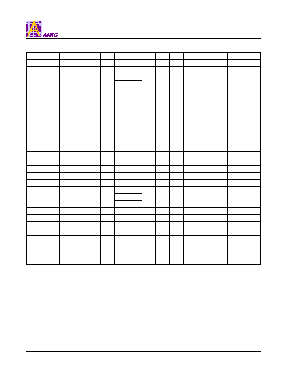
Table 5. A29DL323 Top Boot Sector Group Address Table
Sector Group
A20
A19
A18
A17 A16
A15
A14 A13
A12
Size
Sector
SGA0
0
0
0
0
0
0
X
X
X
64 KB (1 Sector)
FSA0
0
1
1
0
SGA1
0
0
0
0
1
1
X
X
X
192 KB (3 Sectors)
FSA1≠FSA3
SGA2
0
0
0
1
X
X
X
X
X
256 KB (4 Sectors)
FSA4≠FSA7
SGA3
0
0
0
1
X
X
X
X
X
256 KB (4 Sectors)
FSA8≠FSA11
SGA4
0
0
1
1
X
X
X
X
X
256 KB (4 Sectors)
FSA12≠FSA15
SGA5
0
1
0
0
X
X
X
X
X
256 KB (4 Sectors)
FSA16≠FSA19
SGA6
0
1
0
1
X
X
X
X
X
256 KB (4 Sectors)
FSA20≠FSA23
SGA7
0
1
1
0
X
X
X
X
X
256 KB (4 Sectors)
FSA24≠FSA27
SGA8
0
1
1
1
X
X
X
X
X
256 KB (4 Sectors)
FSA28≠FSA31
SGA9
0
1
1
1
X
X
X
X
X
256 KB (4 Sectors)
FSA32≠FSA35
SGA10
1
0
0
1
X
X
X
X
X
256 KB (4 Sectors)
FSA36≠FSA39
SGA11
1
0
1
0
X
X
X
X
X
256 KB (4 Sectors)
FSA40≠FSA43
SGA12
1
0
1
1
X
X
X
X
X
256 KB (4 Sectors)
FSA44≠FSA47
SGA13
1
1
0
0
X
X
X
X
X
256 KB (4 Sectors)
FSA48≠FSA51
SGA14
1
1
0
1
X
X
X
X
X
256 KB (4 Sectors)
FSA52≠FSA55
SGA15
1
1
1
0
X
X
X
X
X
256 KB (4 Sectors)
FSA56≠FSA59
0
0
0
1
SGA16
1
1
1
1
1
0
X
X
X
192 KB (3 Sectors)
FSA60≠FSA62
SGA17
1
1
1
1
1
1
0
0
0
8 KB (1 Sector)
FSA63
SGA18
1
1
1
1
1
1
0
0
1
8 KB (1 Sector)
FSA64
SGA19
1
1
1
1
1
1
0
1
0
8 KB (1 Sector)
FSA65
SGA20
1
1
1
1
1
1
0
1
1
8 KB (1 Sector)
FSA66
SGA21
1
1
1
1
1
1
1
0
0
8 KB (1 Sector)
FSA67
SGA22
1
1
1
1
1
1
1
0
1
8 KB (1 Sector)
FSA68
SGA23
1
1
1
1
1
1
1
1
0
8 KB (1 Sector)
FSA69
SGA24
1
1
1
1
1
1
1
1
1
8 KB (1 Sector)
FSA70
Remark X: V
IH
or V
IL
A29DL323 Series
PRELIMINARY (May, 2002, Version 0.0)
13
AMIC Technology, Inc.
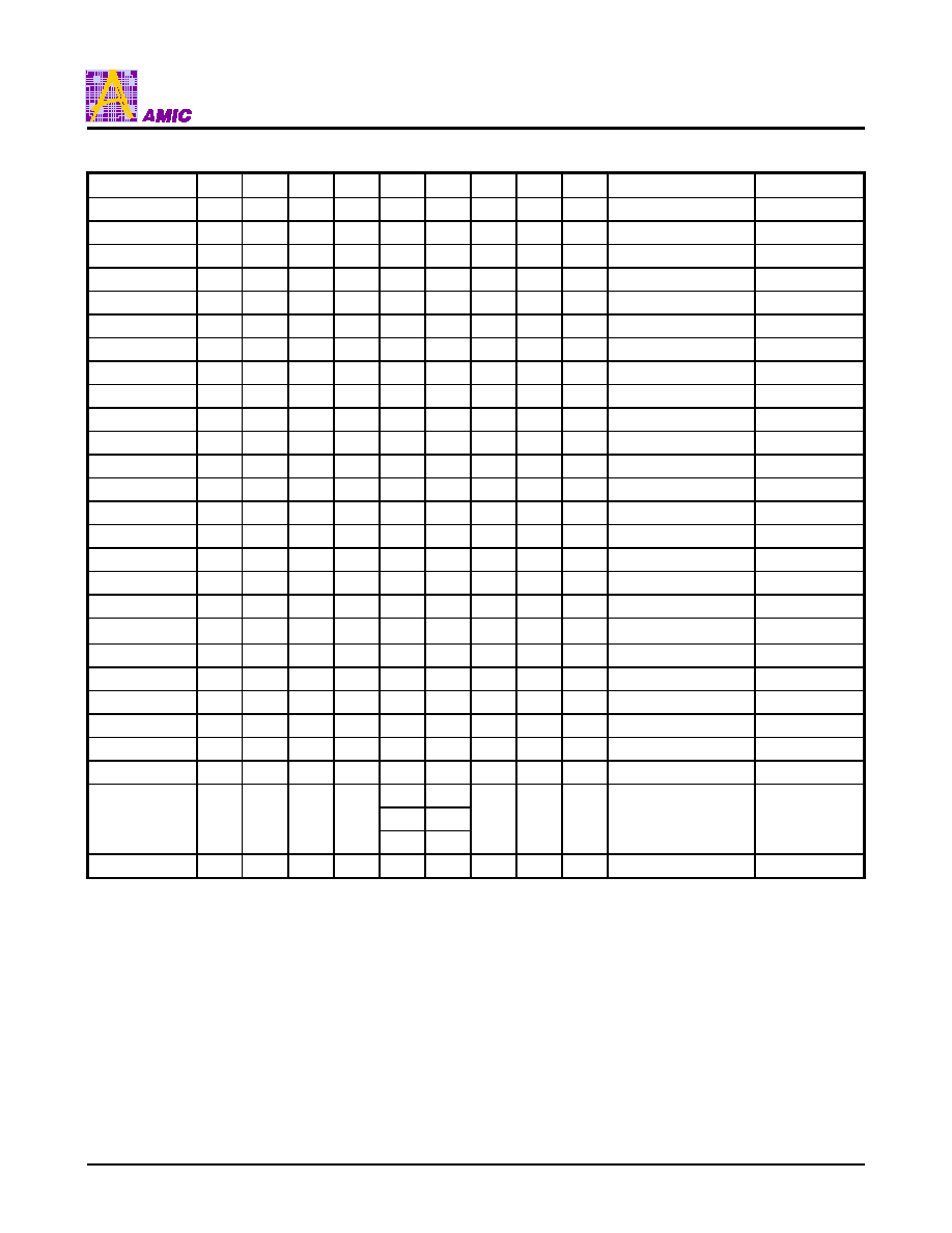
Table 6. A29DL323 Bottom Boot Sector Group Address Table
Sector Group
A20
A19
A18
A17 A16
A15
A14 A13
A12
Size
Sector
SGA0
0
0
0
0
0
0
0
0
0
8 KB (1 Sector)
FSA0
SGA1
0
0
0
0
0
0
0
0
1
8 KB (1 Sector)
FSA1
SGA2
0
0
0
0
0
0
0
1
0
8 KB (1 Sector)
FSA2
SGA3
0
0
0
0
0
0
0
1
1
8 KB (1 Sector)
FSA3
SGA4
0
0
0
0
0
0
1
0
0
8 KB (1 Sector)
FSA4
SGA5
0
0
0
0
0
0
1
0
1
8 KB (1 Sector)
FSA5
SGA6
0
0
0
0
0
0
1
1
0
8 KB (1 Sector)
FSA6
SGA7
0
0
0
0
0
0
1
1
1
8 KB (1 Sector)
FSA7
SGA8
0
0
0
0
0
1
X
X
X
192 KB (3 Sectors)
FSA8≠FSA10
1
0
1
1
SGA9
0
0
0
1
X
X
X
X
X
256 KB (4 Sectors)
FSA11≠FSA14
SGA10
0
0
1
0
X
X
X
X
X
256 KB (4 Sectors)
FSA15≠FSA18
SGA11
0
0
1
1
X
X
X
X
X
256 KB (4 Sectors)
FSA19≠FSA22
SGA12
0
1
0
0
X
X
X
X
X
256 KB (4 Sectors)
FSA23≠FSA26
SGA13
0
1
0
1
X
X
X
X
X
256 KB (4 Sectors)
FSA27≠FSA30
SGA14
0
1
1
0
X
X
X
X
X
256 KB (4 Sectors)
FSA31≠FSA34
SGA15
0
1
1
1
X
X
X
X
X
256 KB (4 Sectors)
FSA35≠FSA38
SGA16
1
0
0
0
X
X
X
X
X
256 KB (4 Sectors)
FSA39≠FSA42
SGA17
1
0
0
1
X
X
X
X
X
256 KB (4 Sectors)
FSA43≠FSA46
SGA18
1
0
1
0
X
X
X
X
X
256 KB (4 Sectors)
FSA47≠FSA50
SGA19
1
0
1
1
X
X
X
X
X
256 KB (4 Sectors)
FSA51≠FSA54
SGA20
1
1
0
0
X
X
X
X
X
256 KB (4 Sectors)
FSA55≠FSA58
SGA21
1
1
0
1
X
X
X
X
X
256 KB (4 Sectors)
FSA59≠FSA62
SGA22
1
1
1
0
X
X
X
X
X
256 KB (4 Sectors)
FSA63≠FSA66
0
0
0
1
SGA23
1
1
1
1
1
0
X
X
X
192 KB (3 Sector)
FSA67≠FSA69
SGA24
1
1
1
1
1
1
X
X
X
64 KB (1 Sector)
FSA70
Remark X: V
IH
or V
IL
A29DL323 Series
PRELIMINARY (May, 2002, Version 0.0)
14
AMIC Technology, Inc.
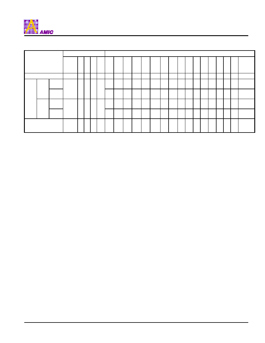
Table 7. A29DL323 Product ID Code (Manufacture Code / Device Code)
Input
Output
Product ID Code
A12
to
A20
A6 A1 A0 A-1
Note
1
I/O
15
I/O
14
I/O
13
I/O
12
I/O
11
I/O
10
I/O
9
I/O
8
I/O
7
I/O
6
I/O
5
I/O
4
I/O
3
I/O
2
I/O
1
I/O
0
HEX
Manufacturer Code
X
V
IL
V
IL
V
IL
V
IL
0
0
0
0
0
0
0
0
0
0
0
1
0
0
0
0
10H
Top
Boot
Hi-Z Hi-Z Hi-Z Hi-Z Hi-Z Hi-Z Hi-Z Hi-Z 0
1
0
1
0
0
0
0
50H
BYTE
mode
Bottom
Boot
X
V
IL
V
IL
V
IL
V
IL
Hi-Z Hi-Z Hi-Z Hi-Z Hi-Z Hi-Z Hi-Z Hi-Z 0
1
0
1
0
0
1
1
53H
Top
Boot
0
0
1
0
0
0
1
0
0
1
0
1
0
0
0
0
2250H
Device
Code
WOR
D
mode Bottom
Boot
X
V
IL
V
IL
V
IH
X
0
0
1
0
0
0
1
0
0
1
0
1
0
0
1
1
2253H
Sector Group
Protection
Sector
Group
Address
V
IL
V
IH
V
IL
V
IL
0
0
0
0
0
0
0
0
0
0
0
0
0
0
0
1 01H
Note2
Notes: 1. A-1 is valid only in the BYTE mode. I/O
8
to I/O
14
go into a high-impedance state in the BYTE mode, and I/O
15
is A-1 of
the lowest address.
2. If 01H is output, the sector group is protected. If 00H is output, the sector group is unprotected.
Remark X: V
IH
or V
IL

A29L323 Series
PRELIMINARY (May, 2002, Version 0.0)
15
AMIC Technology, Inc.
Sector Group Protection
This command performs sector group protection.
By applying V
ID
to RESET and writing 60H to any address,
the device enters the sector group protection mode.
Sector group protection is started by inputting the sector
group address of the sector group to be protected to A12 to
A20, inputting (A6, A1, A0) = (V
IL
, V
IH
, V
IL
), and writing 60H.
After a timeout of 250
µ
s, sector group protection is
completed.
Next, with the sector group address input to A12 to A20, the
device enters the sector group protection verify mode by
inputting (A6, A1, A0) = (V
IL
, V
IH
, V
IL
), and writing 40H. When
read is performed in this state, the sector group protection
verify result is output to I/O0. If "1" is output to I/O0, the
verified sector group is protected. If "1" was not output to
I/O0, sector group protection failed, so perform sector group
protection again.
For the timing waveform and flow chart, refer to Timing
Waveform for Sector Group Protection and Figure 1.
Sector Group Unprotect
This command performs sector group unprotect.
Sector group unprotect is performed for all sector group.
Unprotect cannot be performed for specific sector group.
Moreover, all sector groups must be protected priors to
unprotect.
The device enters the sector group unprotect mode by
applying VID to RESET and writing 60H to any address.
If unprotected sector group exist, first perform sector group
protection for these sector groups. To protect a sector group,
input the sector group address of the sector group to be
protected to the sector group address input pin, input (A6,
A1, A0) = (V
IL
, V
IH
, V
IL
), and write 60H (refer to Sector Group
Protection).
Sector group unprotect is started by inputting (A6, A1, A0) =
(V
IH,
V
IH
, V
IL
), and writing 60H to any address.
Following a timeout of 15 ms, sector group unprotect is
completed.
Unprotect verification must be performed for each sector
group.
The device enters the sector group unprotect verification
mode by inputting the sector group address to input pin of
sector group address and writing 40H, with input (A6, A1, A0)
= (V
IH
, V
IH
, V
IL
).
If reading is performed in this state, the sector group
unprotect verification result is output to I/O
0
. If the verified
sector group is unprotected, "0" is output to I/O
0
. If "0" is not
output to I/O
0
, this means that unprotect failed, so perform
sector group unprotect again.
For the flow chart, refer to Figure 2. Sector Group Unprotect
Flow Chart.
Query
The dual operation flash memory conforms to CFI (Common
Flash memory Interface). CFI enables information about a
device such as the device specifications, memory density,
and supply voltage to be read. Therefore, the software of the
host system can support the software algorithm of a specific
vendor used by a device by using the CFI. For details, refer
to the CFI specifications.
By writing the Query command (98H) and giving an address,
the device information corresponding to that address can be
read. If the device information is read in the WORD mode
(16 bits), the upper bytes of data (I/O
15
to I/O
8
) are "0".
To end the Query mode, writes the read / reset command.
Extra One Time Protect Sector Entry
The dual operation flash memory has a sector area that has
One Time Protect function. This area does not allow code
that has been written to the area to be changed. This area
can be programmed or erased until it is protected.
Once it has been protected, however, protection can never
be canceled. Therefore, care must be exercised when using
this area.
The Extra One Time Protect Sector area has a density of 64
Kbytes and exits at the same addresses as the 8 Kbytes
sector. These addresses are 3F0000H to 3FFFFFH for top
boot in the BYTE mode (1F8000H to 1FFFFFH in the WORD
mode), and 000000H to 00FFFFH for bottom boot in the
BYTE mode (000000H to 007FFFH in the WORD mode).
Because boot block areas (8 Kbytes x 8 sectors) usually
appear in the areas of these addresses, the Extra One Time
Protect Sector entry command sequence must be written to
enter them as the Extra One Time Protect Sector area. The
status in which the Extra One Time Protect Sector area
appears is the Extra One Time Protect Sector mode.
In the Extra One Time Protect Sector mode, the other
sectors, except the boot block area, can be read. In addition,
the Extra One Time Protect Sector area can be read,
programmed, or erased in this mode. To exit from the Extra
One Time Protect Sector mode, the Extra One Time Protect
Sector Reset command sequence must be written.
Extra One Time Protect Sector Program
To program data to the Extra One Time Protect Sector area,
write the Extra One Time Protect Sector Program command
sequence in the Extra One Time Protect Sector mode. This
command is no different from the conventional program
command except that it must be written in the Extra One
Time Protect Sector mode. Therefore, completion of
execution of this command is detected in the same manner
as the conventional detection method of using I/O
7
data
polling, I/O
6
toggle bit, and RY/
BY
. Care must be exercised
in selecting a program destination address. If a program
destination address other than the one in the Extra One Time
Protect Sector area is selected, the data of that address is
changed.

A29DL323 Series
PRELIMINARY (May, 2002, Version 0.0)
16
AMIC Technology, Inc.
Extra One Time Protect Sector Erase
To erase the Extra One Time Protect Sector area, write the
Extra One Time Protect Sector erase command sequence in
the Extra One Time Protect Sector mode. This command is
the same as the conventional sector erase command except
that it must be written in the Extra One Time Protect Sector
mode. Therefore, completion of execution of this command is
detected in the same manner as the conventional detection
method of using I/O
7
data polling, I/O
6
toggle bit, and
RY/
BY
. Care must be exercised in selecting a sector
address to erase. If a sector address other than the one in
the Extra One Time Protect Sector area is selected, the data
of that sector is changed.
Extra One Time Protect Sector Protection
The following write operations are used to protect the Extra
One Time Protect area during the Extra One Time Protect
Sector mode.
Write the sector group protection setup command (60H) in
the Extra One Time Protect Sector mode.
. Set (A6, A1, A0) = (V
IL
, V
IH
, V
IL
), and set the sector address
that selects the Extra One Time Protect Sector.
. Write the sector group protection command (60H).
Because the sequence is the same as the conventional
command sequence to protect a sector group except that the
Extra One Time Protect Sector mode must be set and that
VID is not input to the RESET , the same command
sequence can be used.
For details of how to protect a sector group, refer to Sector
Group Protection.
If an address other than the one of the Extra One Time
Protect Sector area is specified as a sector address, the
other sectors are affected. Once the sector has been
protected, protection can never be canceled. Exercise utmost
care when protecting a sector.
Hardware Data Protection
This device requires two unlock cycles for program / erase
command sequence to prevent illegal program / erase.
Moreover, a hardware data protect function is provided as
follows.
Low VCC Write Inhibit
To prevent an illegal write cycle during VCC transition, the
command register and program / erase circuit is disabled and
all write cycles are ignored while VCC is V
LKO
or lower. Write
commands are ignored until VCC becomes equal to or
greater than V
LKO
.
Logical Inhibit
The write cycle is inhibited under any of the following
conditions :
OE
= V
IL
,
CE
= V
IH
, or
WE
= V
IH
. To start a
write cycle,
CE
= V
IL
and
WE
= V
IL
must be set while /OE =
V
IH
.
Power-Up Write Inhibit
Even if
WE
=
CE
= V
IL
and
OE
= V
IH
are satisfied at
power-up, no commands are accepted at the rising edge of
WE
. The device is automatically reset to the read mode at
power ON.
Write Pulse "Glitch" Protection
Because
OE
,
CE
, and /WE reject a noise pulse of 5 ns
(typical) or less as an invalid pulse, a write operation is not
started.
Sector Group Protection
The dual operation flash memory can be protected by the
user in sector group units. For details, refer to Sector Group
Protection.
A29L323 Series
PRELIMINARY (May, 2002, Version 0.0)
17
AMIC Technology, Inc.
START
RESET=V
ID
Wait 4 us
Protect Sector Group?
Pulse Count=1
Sector Group Protection
(A6, A1, A0)=(V
IL
, V
IH
, V
IL
),
Address=SGA, Data=60H
Timeout 250us
Verify Sector Group Protection
(A6, A1, A0)=(V
IL
, V
IH
, V
IL
),
Address=SGA, Data=40H
Read from Sector Group Address
(A6, A1, A0)=(V
IL
, V
IH
, V
IL
),
Address=SGA
Data=01H?
Protect Other
Sector Group?
Remove V
ID
from RESET,
Write Reset Command
Sector Group Protect Complete
Temporary Sector Group
Unprotect Mode
No
Yes
Yes
No
Yes
Sector Group
Protection (Unprotect) Mode
Address=Don't care
Data=60H
Next Sector Group Address
Increment Pulse Count
Data=01H?
No
No
Remove VID from RESET,
Write Reset Command
Yes
Fail
Figure 1. Sector Group Protection Flow Chart
A29L323 Series
PRELIMINARY (May, 2002, Version 0.0)
18
AMIC Technology, Inc.
START
RESET=V
ID
Wait 4 us
All Sector Group Protected?
Verify Sector Group Protection
(A6, A1, A0)=(V
IL
, V
IH
, V
IL
)
A12 to A20=SGA, Data=40H
Read from Sector Group Address
(A6, A1, A0)=(V
IL
, V
IH
, V
IL
),
A12 to A20=SGA
n=0, Pluse Count=1
Verify Sector Group Protection
(A6, A1, A0)=(V
IH
, V
IH
, V
IL
),
Address=SGA, Data=40H
Read from Sector Group Address
(A6, A1, A0)=(V
IH
, V
IH
, V
IL
),
A12 to A20=SGA
Data=00H?
Last Sector Group (n=25)?
Remove V
ID
from RESET,
Write Reset Command
Sector Group Protect Complete
No
Yes
Yes
Yes
No
n=0
Next Sector Group Address
(n=n+1)
Increment Pulse
Pulse Count=1000?
No
No
Remove VID from RESET,
Write Reset Command
Yes
Fail
Figure 2. Sector Group Unprotect Flow Chart
Sector Group Protection
Address=Don't Care, Data=60H
Data=0H?
Last Sector Group (n=25)?
Yes
Yes
Sector Group Unprotect
(A6, A1, A0)=(V
IH
, V
IH
, V
IL
),
Data=60H
Timeout 15ms
Next Sector Group Address
(n=n+1)
Sector Group Protection
No
Yes
A29L323 Series
PRELIMINARY (May, 2002, Version 0.0)
19
AMIC Technology, Inc.
CFI Code List
Address A6 to A0
Data I/O
15
to I/O
0
Description
10H
11H
12H
0051H
0052H
0059H
"QRY" (ASCII code)
13H
14H
0002H
0000H
Main command set
2 : AMD/FJ standard type
15H
16H
0040H
0000H
Start address of PRIMARY table
17H
18H
0000H
0000H
Auxiliary command set
00H : Not supported
19H
1AH
0000H
0000H
Start address of auxiliary algorithm table
1BH
0027H
Minimum VCC voltage (program / erase)
I/O
7
to I/O
4
: 1 V/bit
I/O
3
to I/O
0
: 100 mV/bit
1CH
0036H
Maximum VCC voltage (program / erase)
I/O
7
to I/O
4
: 1 V/bit
I/O
3
to I/O
0
: 100 mV/bit
1DH
0000H
Minimum VPP voltage
1EH
0000H
Maximum VPP voltage
1FH
0004H
Typical word program time (2
N
µs)
20H
0000H
Typical buffer program time (2
N
µs)
21H
000AH
Typical sector erase time (2
N
ms)
22H
0000H
Typical chip erase time (2
N
ms)
23H
0005H
Maximum word program time (typical time ◊ 2
N
)
24H
0000H
Maximum buffer program time (typical time ◊ 2
N
)
25H
0004H
Maximum sector erasing time (typical time ◊ 2
N
)
26H
0000H
Maximum chip erasing time (typical time ◊ 2
N
)
27H
0016H
Capacity (2
N
Bytes)
28H
29H
0002H
0000H
I/O information
2 : ◊8/◊16-bit organization
2AH
2BH
0000H
0000H
Maximum number of bytes when two banks are programmed (2
N
)
2CH
0002H
Type of erase block
2DH
2EH
2FH
30H
0007H
0000H
0020H
0000H
Information about erase block 1
Bit0 to 15 : y = number of sectors
Bit16 to 31 : z = size
(Z ◊ 256 Bytes)
31H
32H
33H
34H
003EH
0000H
0000H
0001H
Information about erase block 2
bit0 to 15 : y = number of sectors
bit16 to 31 : z = size
(z ◊ 256 Bytes)
40H
41H
42H
0050H
0052H
0049H
"PRI" (ASCII code)
A29DL323 Series
PRELIMINARY (May, 2002, Version 0.0)
20
AMIC Technology, Inc.
CFI Code List (continued)
Address A6 to A0
Data I/O
15
to I/O
0
Description
43H
0031H
Main version (ASCII code)
44H
0032H
Minor version (ASCII code)
45H
0000H
Address during command input
00H : Necessary
01H : Unnecessary
46H
0002H
Temporary erase suspend function
00H : Not supported
01H : Read only
02H : Read / Program
47H
0001H
Sector group protection
00H : Not supported
01H : Supported
48H
0001H
Temporary sector group protection
00H : Not supported
01H : Supported
49H
0004H
Sector group protection algorithm
4AH
00XXH
Number of sectors of bank 2
00H : Not supported
30H : A29DL323
4BH
0000H
Burst mode
00H : Not supported
4CH
0000H
Page mode
00H : Not supported
4DH
0085H
Minimum V
ACC
voltage
I/O
7
to I/O
4
: 1 V/bit
I/O
3
to I/O
0
: 100 mV/bit
4EH
0095H
Maximum V
ACC
voltage
I/O
7
to I/O
4
: 1 V/bit
I/O
3
to I/O
0
: 100 mV/bit
4FH
00XXH
Boot organization
02H : Bottom boot (A29DL323UX-XX)
03H : Top boot (A29DL323TX-XX)
50H
0001H
Temporary program suspend function
00H : Not supported
01H : Supported
A29DL323 Series
PRELIMINARY (May, 2002, Version 0.0)
21
AMIC Technology, Inc.
Command Definitions
Writing Commands
All operations are executed by writing a command.
To write a command, the write cycle of a standard
microprocessor is used.
The operation of the device is controlled by writing a
command to a register. The command register is a function
that latches the address and data necessary for executing an
instruction and does not occupy the memory area.
If an illegal address or data is written or if an address or data
is written in the wrong sequence, the device is reset to the
read mode.
Table 8. shows the commands and command sequences.
Read / Reset Command
This command resets the device to the read mode.
The read mode is maintained until the contents of the
command register are changed.
Once the device is in the read mode, no command is
necessary for reading data. Data read can be performed
using the read cycle of a standard microprocessor.
The read mode is maintained until the contents of the
command register are changed.
Product ID
The manufacturer code and device code can be read without
inputting a high voltage to the address pin.
If a bank address is specified in the third bus cycle and a read
operation is started from address xx00H in the fourth bus
cycle, manufacturer code 10H is output. If address xx02H
(BYTE mode) or xx01H (WORD mode) is read, the device
code is output. If a read operation is executed from an
address in the bank not specified in the third bus cycle, data
of the memory cell is output.
If a read operation is executed starting from address (BA)
02H (WORD mode) or (BA) 04H (BYTE mode), information
indicating which sector group is protected can be obtained. If
the sector group address is scanned with (A6, A1, A0) = (V
IL
,
V
IH
, V
IL
), "1" is output to I/O
0
to indicate that the sector group
is protected (for details refer to Sector Group Protection).
The product ID can be read only from the specified bank. To
read the manufacturer code, device code, and information on
protection of sector group from a bank not specified, write the
read / reset command, specify the bank address to be read,
and then write the product ID command again. To end the
product ID mode, writes the read / reset command. To write
the product ID command in the product ID mode, execute the
read / reset command once.
Program Command Sequence
This command is used to program data.
Program is performed in 1 byte or 1 word units. Program can
be performed regardless of the address sequence, even if the
sector limit is exceeded. However, "0" cannot be changed
back into "1" through the program operation. If overwriting "1"
to "0" is attempted, the program operation is interrupted and
"1" is output to I/O
5
, or successful program is indicated in data
polling, but actually the data is "0" as before.
Following write by command sequence, the pulse required for
program is automatically generated inside the device and
program verification is automatically performed, so that
control from external is not required.
During automatic program, any command other than the
program suspend is ignored. However, automatic program is
interrupted when hardware reset is performed. Since the
programmed data is not guaranteed in this case, reexecute
the program command following completion of reset.
Upon completion of automatic program, the device returns to
the read mode.
The operation status of automatic program can be determined
by using the hardware sequence flags (I/O
7
, I/O
6
, RY/
BY
pins).
See sections "I/O
7
(Data Polling)", "I/O
6
(Toggle Bit)", and
"RY/
BY
(Ready /
Busy
)".
For the timing waveform and flow chart, refer to Timing
Waveform for Write Cycle (
WE
Controlled), Timing
Waveform for Write Cycle (
CE
Controlled) and Figure 3.
START
Write Program
Command
Sequence
Data Poll
from System
Last Address ?
Programming
Completed
No
Yes
Yes
Increment Address
Figure 3. Program Flow Chart
A29DL323 Series
PRELIMINARY (May, 2002, Version 0.0)
22
AMIC Technology, Inc.
Program Suspend / Resume Commands
This command is used to suspend automatic programming.
Addresses not being programmed to while programming is
suspended can be read.
Sector erase (including the timeout period) and data program
operations can be both suspended. Chip erase operations
cannot be suspended.
1
µ
s is required between when the command sequence is
programmed and when the automatic program operation is
suspended.
The execution status of an automatic program operation can
be determined using a hardware sequence flag (I/O
7
, I/O
6
pins.) refer to I/O
7
(Data polling) and I/O
6
(Toggle Bit).
To resume an automatic program operation, write the resume
command (30H) while the operation is suspended.
Caution about Program Suspend / Resume Commands
If automatic program resume and suspend are repeated at
intervals of less than 5
µ
s, the program operation may not be
correctly completed.
Chip Erase Command Sequence
This command is used to erase the entire chip.
Following command sequence write, erase is performed
after "0" is written to all memory cells and verification is
performed, using the automatic erase function. Program
before erase and control from external are not required.
During automatic erase, all commands that have been
written are ignored. However, automatic erase is
interrupted by hardware reset. Since erase is not
guaranteed in this case, execute the chip erase
command again after reset is completed.
Upon completion of automatic erase, the device returns
to read mode.
The automatic erase operation status can be determined
with the hardware sequence flags (I/O
7
, I/O
6
, RY/
BY
pins).
See sections "I/O
7
(Data Polling)", "I/O
6
(Toggle Bit)",
and "RY/
BY
(Ready /
Busy
)".
For the timing waveform and flow chart, refer to Timing
Waveform for Sector / Chip Erase and Figure 4.
Sector Erase Command Sequence
This command is used to erase data in sector units.
"0" is written to the entire sector whose data is to be erased by
the automatic erase function after the command sequence has
been written, and erase is executed after verification has been
performed. Programming before erase and external control are
not necessary.
The timeout period of sector erase starts when erase
command 30H and the address of the sector to be erased are
written at the sixth bus cycle. When this timeout period (50
µ
s)
has elapsed, the device automatically starts erasing.
Two or more sectors can be selected and erased at the same
time by additionally writing erase command 30H and the
address of the sector whose data is to be erased during the
timeout period. In this case, the timeout period starts again
after the last erase command has been written.
If a protected sector and a sector that is not protected are
included in the selected sectors, only the sector that is not
protected is erased and the protected sector is ignored.
If a command other than the sector erase or erase suspend
command is input during the timeout period, the device is reset
to the read mode. If the timeout period has elapsed and erase
has started, any command other than the erase suspend
command is ignored. However, erase is stopped if hardware
reset is executed. In this case, sector erase is not guaranteed.
Execute the sector erase command again after completion of
reset.
When automatic erasure has been completed, the device
returns to the read mode.
Completion of automatic sector erase can be reported to the
host system by using the data polling function of I/O
7
, toggle
bit function of I/O
6
, and RY/ BY pin. Sector erase is started
after the lapse of the timeout period that is started from the
rising of the
WE
or
CE
pulse, whichever earlier, of the last
sector erase command and is completed when the data of I/O
7
is set to "1" (refer to Hardware Sequence Flags). The device
returns to the read mode. Data polling and toggle bit function
in any address of the sector that is to be erased. The time
required to erase two or more sectors is "(sector programming
time + sector erase time) x number of sectors". If two or more
sectors of different banks are erased, a read operation from a
bank (i.e., dual operation) cannot be executed.
For the timing waveform and flow chart, refer to Timing
Waveform for Sector / Chip Erase and Figure 4.
START
Write Erase
Command
Sequence
Data Poll
from System
Data = FFh ?
Erasure Completed
Yes
No
Figure 4. Sector / Chip Erase Flow Chart
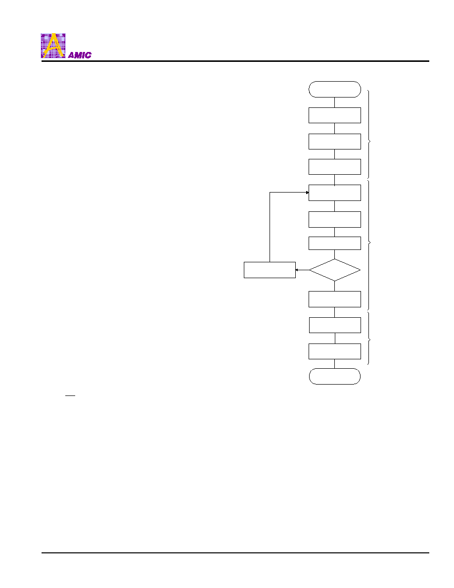
A29DL323 Series
PRELIMINARY (May, 2002, Version 0.0)
23
AMIC Technology, Inc.
Sector Erase Suspend / Resume Commands
This command suspends automatic erase. During erase
suspend, sectors for which erase is not performed can be read
and programmed.
Sector erase (including the timeout period) and data program
operations can be both be suspended. Chip erase operations
cannot be suspended. Suspend can be performed for all
sectors for which erase is being performed.
Following command sequence write, 20
µ
s are required until
automatic erase is suspended.
While automatic erase is suspended, any sector for which
erase is not being performed can be read and programmed.
Whether automatic erase is suspended can be determined
with the hardware sequence flags (I/O
7
, I/O
6
, I/O
2
pins). See
sections "I/O7 (Data Polling)", "I/O6 (Toggle Bit)", and "I/O2
(Toggle Bit II)".
If resume automatic erase that has been suspended, write the
resume command (30H) while sector erase is suspended. At
this time, input a bank address of the sector for which erasure
is suspended.
Caution Sector Erase Suspend / Resume Commands
If automatic erase resume and suspend are repeated at
intervals of less than 100
µ
s, the erasure operation may not be
correctly completed.
Unlock Bypass Command Sequence
This device provides an unlock bypass mode to shorten the
program time.
Normally, 4 write cycle included with 2 unlock cycles are
required during program. In contrast, with the unlock bypass
mode, it is possible to perform program without unlock cycles.
In the unlock bypass mode, all commands except unlock
bypass program and unlock bypass reset are ignored.
To end the unlock bypass mode, the unlock bypass reset
command must be written. Note, however, that the unlock
bypass reset command must be written to an address of the
bank that is not being read in dual operation. If the unlock
bypass reset command is written, the device returns to the
normal read mode.
In the unlock bypass mode, the operating current is necessary
even if
CE
= V
IH
.
For the flowchart, refer to Figure 5.
Unlock Bypass Set
This command sets the device to the unlock bypass mode.
Unlock Bypass Program
This command is used to perform program in the unlock
bypass mode.
Unlock Bypass Reset
This command is used to quit the unlock bypass mode.
When this command is executed, the device returns to the
read mode.
START
Address=555H
Data=AAH
Address=2AAH
Data=55H
Last Address ?
End
No
Yes
Figure 5. Unlock Bypass Flow Chart (WORD Mode)
Address=Don't Care
Data=A0H
Address=Program Address
Data=Program Data
Data Polling
Programming Completed
Address=Don't Care
Data=00H
Note: This flow chart shows the WORD mode's case. In the BYTE
mode, address to be input is different from the WORD mode.
See Table 8. Command Sequence
Address=555H
Data=20H
Address=BA
Data=90H
Unlock Bypass Set
Unlock Bypass Program
Unlock Bypass Reset
Next Address
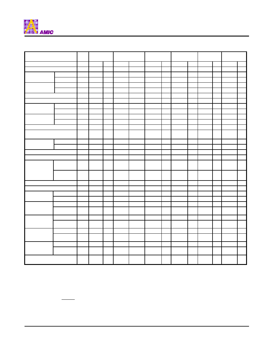
A29L323 Series
PRELIMINARY (May, 2002, Version 0.0)
24
AMIC Technology, Inc.
Table 8. A29DL323 Command Sequence
Command Sequence
Bus
Cycle
1
st
Bus Cycle
2
nd
Bus Cycle
3
rd
Bus Cycle 4
th
Bus Cycle 5
th
Bus Cycle 6
th
Bus Cycle
Address Data Address
Data
Address Data Address Data Address Data Address Data
Read / Reset
Note 1
1
XXXH F0H
RA
RD
-
-
-
-
-
-
-
-
BYTE mode
3
AAAH AAH
555H
55H
AAAH
F0H
RA
RD
-
-
-
-
Read / Reset
Note 1
WORD mode
555H
2AAH
555H
BYTE mode
4
AAAH AAH
555H
55H
AAAH
A0H
PA
PD
-
-
-
-
Program
WORD mode
555H
2AAH
555H
Program Suspend
Note2
1
BA
B0H
-
-
-
-
-
-
-
-
-
-
Program Suspend
Note3
1
BA
30H
-
-
-
-
-
-
-
-
-
-
BYTE mode
6
AAAH AAH
555H
55H
AAAH
80H
AAAH AAH 555H 55H AAAH 10H
Chip Erase
WORD mode
555H
2AAH
555H
555H
2AAH
555H
BYTE mode
6
AAAH AAH
555H
55H
AAAH
80H
AAAH AAH 555H 55H
FSA
30H
Sector Erase
WORD mode
555H
2AAH
555H
555H
2AAH
Sector Erase Suspend
Note4
1
BA
B0H
-
-
-
-
-
-
-
-
-
-
Sector Erase Suspend Resume
Note5
1
BA
30H
-
-
-
-
-
-
-
-
-
-
BYTE mode
3
AAAH AAH
555H
55H
AAAH
20H
-
-
-
-
-
-
Unlock Bypass
Set
WORD mode
555H
2AAH
555H
Unlock Bypass Program
Note6
2
XXXH A0H
PA
PD
-
-
-
-
-
-
-
-
Unlock Bypass Reset
Note7
2
BA
90H
XXXH 00H
Note11
-
-
-
-
-
-
-
-
BYTE mode
3
AAAH AAH
555H
55H
(BA)
AAAH
90H
IA
ID
-
-
-
-
Product ID
WORD mode
555H
2AAH
(BA)
555H
Sector Group Protection
Note7
4
XXXH 60H
SPA
60H
SPA
40H
SPA
SD
-
-
-
-
Sector Group Unprotect
Note8
4
XXXH 60H
SUA
60H
SUA
40H
SUA
SD
-
-
-
-
BYTE mode
1
AAH
98H
-
-
-
-
-
-
-
-
-
-
Query
Note9
WORD mode
55H
BYTE mode
3
AAAH AAH
555H
55H
AAAH
88H
-
-
-
-
-
-
Extra One Time
Protect Sector
Entry
WORD mode
555H
2AAH
555H
BYTE mode
4
AAAH AAH
555H
55H
AAAH
A0H
PA
PD
-
-
-
-
Extra One Time
Protect Sector
Program
Note10
WORD mode
555H
2AAH
555H
BYTE mode
6
AAAH AAH
555H
55H
AAAH
80H
AAAH AAH 555H 55H EOTPSA 30H
Extra One Time
Protect Sector
Erase
Note10
WORD mode
555H
2AAH
555H
555H
2AAH
BYTE mode
4
AAAH AAH
555H
55H
AAAH
90H
XXXH
00H
-
-
-
-
Extra One Time
Protect Sector
Reset
Note10
WORD mode
555H
2AAH
555H
Extra One Time Protect Sector
Protection
Note10
4
XXXH 60H EOTPSA
60H
EOTPSA 40H EOTPSA SD
-
-
-
-
Note:
1. Both these read / reset commands reset the device to the read mode.
2. Programming is suspended if B0H is input to the bank address being programmed to in a program operation.
3. Programming is resumed if 30H is input to the bank address being suspended to in a program-suspend operation.
4. Erasure is suspended if B0H is input to the bank address being erased in a sector erase operation.
5. Erasure is resumed if 30H is input to the bank address being suspended in a sector-erase-suspend operation.
6. Valid only in the unlock bypass mode.
7. Valid only when RESET = V
ID
(except in the Extra One Time Protect Sector mode).
8. The command sequence that protects a sector group is excluded.

A29DL323 Series
PRELIMINARY (May, 2002, Version 0.0)
25
AMIC Technology, Inc.
9. Only A0 to A6 are valid as an address.
10. Valid only in the Extra One Time Protect Sector mode.
11. This command can be used even if this data is F0H.
Remarks:
1. Specify address 555H or 2AAH (A10 to A0) in the WORD mode, and AAAH or 555H (A10 to A0, A-1) in the BYTE mode.
2. RA : Read address
RD : Read data
IA : Address input
xx00H (to read the manufacturer code)
xx02H (to read the device code in the BYTE mode)
xx01H (to read the device code in the WORD mode)
ID : Code output. Refer to the Product ID code (Manufacturer code / Device code).
PA : Program address
PD : Program data
FSA: Erase sector address. The sector to be erased is selected by the combination of this address.
Refer to the Sector Organization / Sector Address Table.
BA : Bank address. Refer to the Sector Organization / Sector Address Table.
SPA : Sector group address to be protected. Set sector group address (SGA) and (A6, A1, A0) = (V
IL
, V
IH
, V
IL
).
SUA : Unprotect sector group address. Set sector group address (SGA) and (A6, A1, A0) = (V
IH
, V
IH
, V
IL
).
EOTPSA : Extra One Time Protect Sector area addresses. These addresses are 3F0000H to 3FFFFFH (BYTE mode) /
1F8000H to 1FFFFFH (WORD mode) for top boot, and 000000H to 00FFFFH (BYTE mode) / 000000H to
007FFFH (WORD mode) for bottom boot.
SD : Data for verifying whether sector groups read from the address specified by SPA, SUA, and EOTPSA are protected or
unprotected.
3. The sector group address is don't care except when a program / erase address or read address are selected.
4.
◊
of address bit indicates V
IH
or V
IL
.
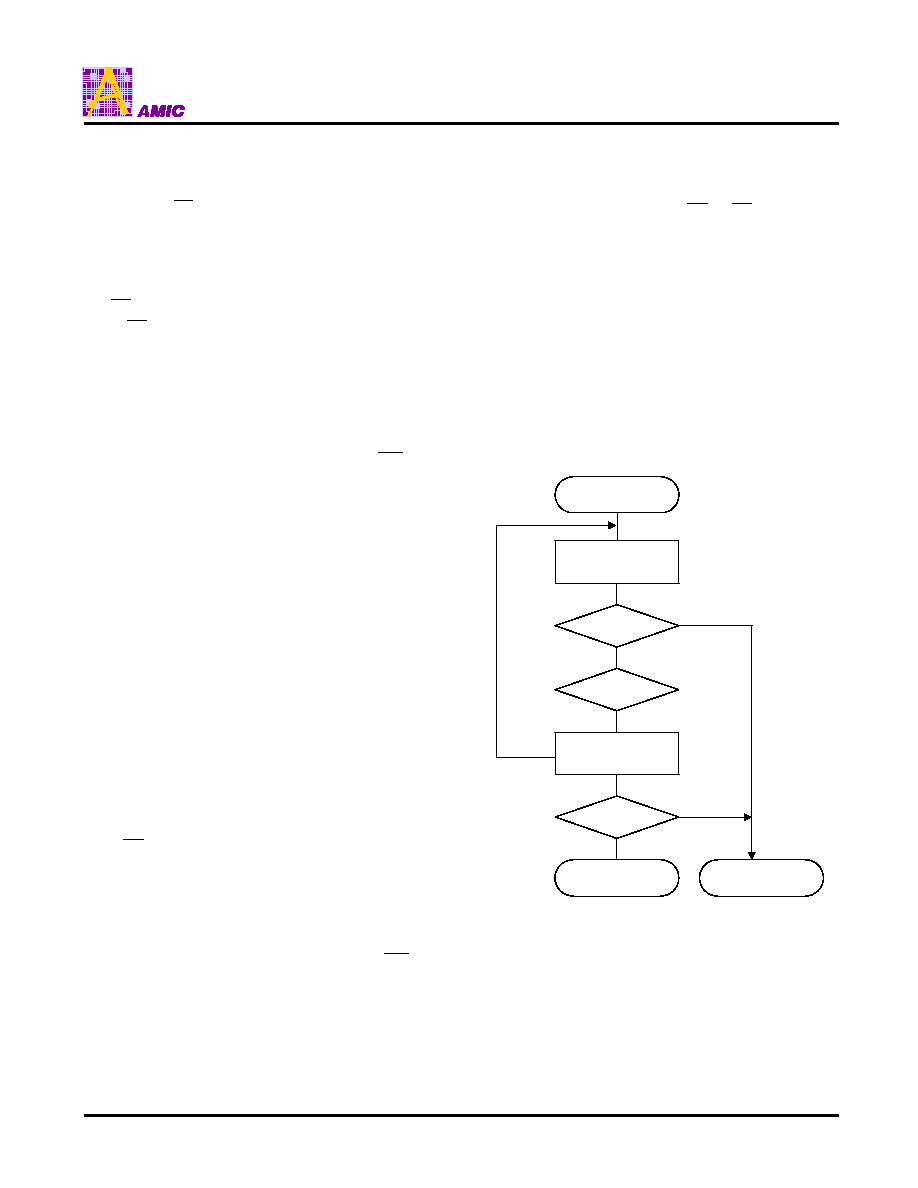
A29DL323 Series
PRELIMINARY (May, 2002, Version 0.0)
26
AMIC Technology, Inc.
Hardware Sequence Flags
The status of automatic program / erase operations can be
determined from the status of the I/O2, I/O3, I/O5, I/O6,
I/O7, and RY /
BY
pins.
Caution When Reading Flags
When checking the completion or suspension status of an
automatic program / erase operation by reading different
sector data within the same bank, be sure to either clock
the
CE
or change the address before reading the data.
If the
CE
is fixed to V
IL
or data is read from the same
address without the address being changed, the output
data may not be output correctly.
I/O
7
: Data Polling
Data polling is a function to determine the status of
automatic program / erase is currently being performed by
using I/O
7
.
Data polling is valid from the rise of the last
WE
in the
program / erase command sequence.
The status of automatic program is currently being
executed can be determined by reading from the program
destination addresses. While automatic programming is
being executed or while automatic programming is being
executed during erasure suspension, the complement of
the final data programmed will be output to I/O
7
. Upon
completion of automatic program, the true value of the
programmed data, not the complement, is output.
The status of automatic erase is in progress can be
determined by reading from the addresses of the sector
being erased. If erase is in progress, "0" is output to I/O
7
. If
the automatic erase operation is complete or if it is
suspend, "1" will be output to I/O
7
when a sector for which
erasure is suspended is read.
During automatic erase, if all the selected sectors are
protected, data polling is valid for approximately 400
µ
s.
The device is then reset to the read mode. If the selected
sectors include protected and unprotected sectors, only
unprotected sectors are erased, and protected sectors are
ignored.
Upon completion of automatic program / erase, after the
data output to I/O
7
changes from the complement to the
true value, I/O
7
changes asynchronously like I/O
0
to I/O
6
while
OE
is maintained at low level.
For the timing waveform and flow chart, refer to Timing
Waveform for Data Polling and Figure 6.
I/O
6
: Toggle Bit
The toggle bit is a function that uses I/O
6
to determine the
status of automatic program / erase is in progress.
The toggle bit is valid from the rise of the last
WE
in the
program / erase command sequence.
If a continuous read is performed from any address of a
bank that is undergoing automatic program or erase, I/O
6
will be toggled. If a sector other than the erased sector is
read after automatic program / erase is complete or when it
is suspended, the I/O
6
toggle operation is stopped, and valid
data for the read is output. If a sector for which erasure is
suspended is read, "1" will be output to I/O
6
. Continuous
read control is performed with the
OE
or
CE
.
If program is performed for an address inside a protected
sector, I/O
6
is toggled approximately 1
µ
s, and then the
device is reset to the read mode.
Moreover, if all the sectors selected at the time of automatic
erase are protected, I/O
6
is toggled approximately 400
µ
s,
and then the device is reset to the read mode.
In this way, by using I/O
6
, it is possible to determine the
status of automatic erase is in progress (or suspended), but
to determine which sector is being erased, I/O
2
(Toggle Bit
II) is used. See section "I/O
2
(Toggle Bit II)".
For the timing waveform and flow chart, refer to Timing
Waveform for Toggle Bit, Timing Waveform for I/O
2
vs. I/O
6
and Figure 7.
I/O
7
=Data?
START
Read (I/O
0
to I/O
7
)
An=Valid Address
I/O
7
=Data?
FAIL
No
Read (I/O
0
to I/O
7
)
An=Valid Address
I/O
5
=1?
Yes
No
PASS
Yes
Yes
Figure 6. Data Polling Flow Chart
No
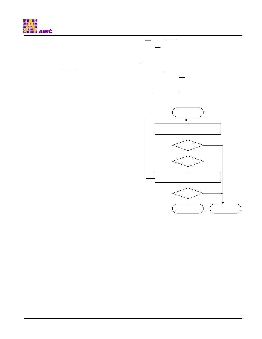
A29L323 Series
PRELIMINARY (May, 2002, Version 0.0)
27
AMIC Technology, Inc.
I/O
2
: Toggle Bit II
Toggle bit II is a function that determines the status of
automatic erase (or erase suspend) is in progress for a
particular sector by using I/O
2
.
I/O
2
is toggled when continuous read is performed from
addresses in a sector during automatic erase (or erase
suspend). Either
OE
or
CE
is used to control continuous
read.
When program to a sector that is not subject to erase
suspend is attempted during erase suspend, read from
sectors that are not subject to erase suspend cannot be
performed until program is completed. In this case, "1" will
be output to I/O
2
if a continuous read is performed from an
address in a sector other than an erased sector.
In this way, it is possible to determine the status of
automatic erase (including erase suspend) is in progress for
sectors specified using I/O
2
, but whether the state is erase in
progress or erase suspend cannot be determined with I/O
2
.
To determine this, I/O
6
(Toggle Bit) must be used. See
section "I/O
6
(Toggle Bit)".
For the timing waveform, refer to Timing Waveform for I/O
2
vs. I/O
6
.
I/O5 : Exceeding Timing Limits
If the program / erase time exceeds the prescribed number
of pulses during automatic program / erase (exceeding
timing limit), "1" is output to I/O
5
and automatic program /
erase failure is indicated.
Moreover, if overwriting "0" to "1" is attempted, the device
judges data overwrite to be impossible, and "1" is output to
I/O
5
when the timing limit is exceeded.
When this happens, execute command reset.
I/O3 : Sector Erase Timer
A 50
µ
s timeout period occurs following write with the sector
erase command sequence before automatic erase starts.
During this timeout period, "0" is output to I/O
3
. When
automatic erase starts upon completion of the timeout
period, "1" is output to I/O
3
.
If sector erase is performed, first confirm whether the device
has received a command by using I/O
7
(Data Polling) or I/O
6
(Toggle Bit). Then, using I/O
3
, check whether automatic
erase has started. If I/O
3
is "0", the timeout period is not
over, and so it is possible to add sectors to erase. If I/O
3
is
"1", automatic erase starts and other commands (except
erase suspend) are ignored until erase is completed.
If a sector to erase is added during the sector erase timeout
period, it is recommended to check I/O
3
prior to and
following the addition. If I/O
3
is "1" following the addition,
that addition may not be accepted.
RY
BY : Read/Busy
The RY/
BY
is a dedicated output pin used to check the
status of automatic program / erase is in progress.
During automatic program / erase, "0" is output to the RY
/
BY
. If "1" is output, this signifies that the device is either in
the read mode (including erase suspend) or standby mode.
Since the RY/
BY
is an open-drain output pin, it is possible
to connect several RY/
BY
in series by connecting a pull-up
resistor to VCC.
For the timing waveform, refer to Timing Waveform for
RY/
BY
(Ready /
Busy
).
I/O
7
=Toggle?
START
Read (I/O
0
to I/O
7
)
An=Any Address in the Bank Being Executed
I/O
7
=Toggle?
FAIL
No
Read (I/O
0
to I/O
7
)
An=Any Address in the Bank Being Executed
I/O
5
=1?
Yes
No
PASS
Yes
No
Figure 7. Toggle Bit Flow Chart
No
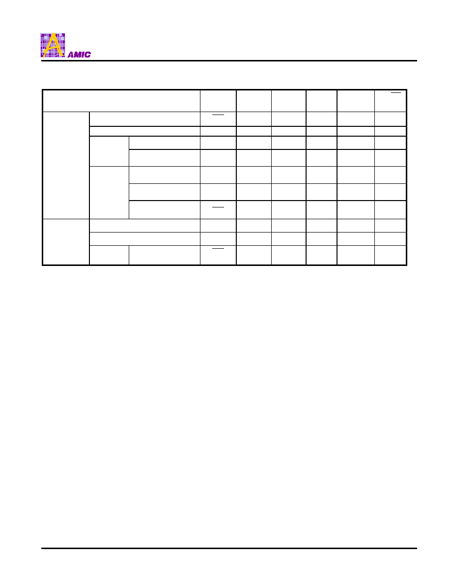
A29DL323 Series
PRELIMINARY (May, 2002, Version 0.0)
28
AMIC Technology, Inc.
Table 9. Hardware Sequence Flags
I/O
7
I/O
6
I/O
5
I/O
3
I/O
2
RY/
BY
Status
(Note 1)
(Note 2)
(Note 3)
(Note 1)
Program
7
I/O
Toggle
0
0
1
0
Erase
0
Toggle
0
1
Toggle
0
Program Sector
Data
Data
Data
Data
Data
Data
Program
Suspend
Other than Program
Sector
Data
Data
Data
Data
Data
1
Erase Suspend
Sector
1
1
0
0
Toggle
1
Other than Erase
Suspend Sector
Data
Data
Data
Data
Data
1
Progress
Erase
Suspend
Erase Suspend
Program
7
I/O
Toggle
0
0
1
0
Program
0
Toggle
1
0
1
0
Erase
0
Toggle
1
1
N/A
0
Exceeding
time limits
Erase
Suspend
Erase Suspend
Program
7
I/O
Toggle
1
0
N/A
0
Notes:
1. To read I/O
7
or I/O
2
, a valid address must be input.
2. To read I/O
6
, any address can be used.
3. For I/O
5
, "1" is output if the automatic program / erase time exceeds the prescribed number of internal pulses.
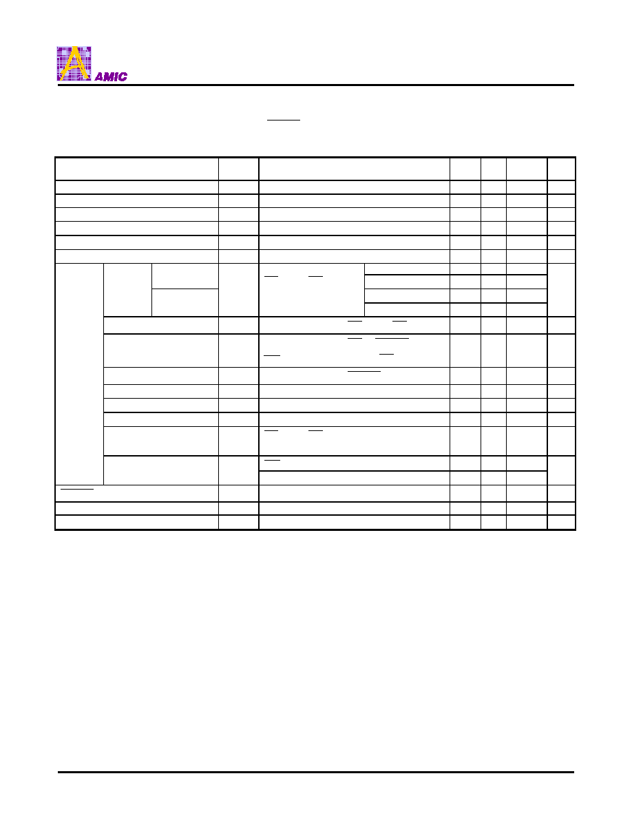
A29DL323 Series
PRELIMINARY (May, 2002, Version 0.0)
29
AMIC Technology, Inc.
Electrical Characteristics
Before turning on power, input GND ± 0.2 V to the
RESET
pin until VCC VCC (MIN.).
DC Characteristics (Recommended Operating Conditions Unless Otherwise Noted)
Parameter
Symbol
Test Description
Min. Typ.
Max.
Unit
High level input voltage
V
IH
2.4
VCC+0.3 V
Low level input voltage
V
IL
-0.3
+0.5
V
High level output voltage
V
OH
I
OH
= -500 µA, VCC = VCC (min.)
2.4
V
Low level output voltage
V
OL
I
OL
= +1.0 mA, VCC = VCC (min.)
0.4
V
Input leakage current
I
LI
-1.0
+1.0
µA
Output leakage current
I
LO
-1.0
+1.0
µA
t
CYCLE
= 5 MHz
10
16
BYTE mode
t
CYCLE
= 1 MHz
2
4
t
CYCLE
= 5 MHz
10
16
Read
WORD mode
I
CC1
VCC = VCC (max.),
CE
= V
IL
,
OE
= V
IH
t
CYCLE
= 1 MHz
2
4
mA
Program, Erase
I
CC2
VCC = VCC (max.),
CE
= V
IL
,
OE
= V
IH
15
30
mA
Standby
I
CC3
VCC = VCC (max.),
CE
=
RESET
=
WP
(ACC) = VCC ± 0.3 V,
OE
= V
IL
0.2
5
µA
Standby / Reset
I
CC4
VCC = VCC (max.),
RESET
= GND ± 0.2 V
0.2
5
µA
Automatic sleep mode
I
CC5
V
IH
= VCC ± 0.2 V, V
IL
= GND ± 0.2 V
0.2
5
µA
Read during programming
I
CC6
V
IH
= VCC ± 0.2 V, V
IL
= GND ± 0.2 V
21
45
mA
Read during erasing
I
CC7
V
IH
= VCC ± 0.2 V, V
IL
= GND ± 0.2 V
21
45
mA
Programming during
suspend
I
CC8
CE
= V
IL
,
OE
= V
IH
,
Automatic programming during suspend
17
35
mA
WP
(ACC) pin
5
10
Power
Supply
Current
Accelerated programming
I
ACC
VCC
15
30
mA
RESET
high level input voltage
V
ID
High Voltage is applied
11.5
12.5
V
Accelerated programming voltage
V
ACC
High Voltage is applied
8.5
9.5
V
Low VCC lock-out voltage (Note)
V
LKO
V
IH
= VCC
±
0.3V
; V
IL
= VSS
±
0.3V
1.7
V
Notes:
1. When VCC is equal to or lower than V
LKO
, the device ignores all write cycles.
Remark: These DC characteristics are in common regardless of product classification.
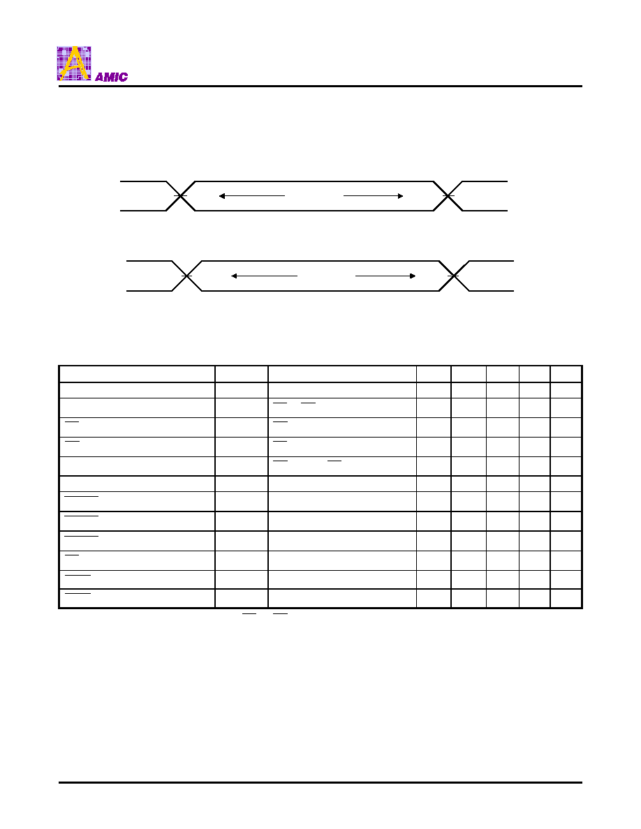
A29L323 Series
PRELIMINARY (May, 2002, Version 0.0)
30
AMIC Technology, Inc.
AC Characteristics (Recommended Operating Conditions Unless Otherwise Noted)
AC Test Conditions
Input Waveform (Rise and Fall Time 5 ns)
3.0V
0V
1.5V
1.5V
Test points
Output Waveform
1.5V
1.5V
Test points
Output Load
1 TTL + 30pF
Read Cycle
Parameter
Symbol
Test Condition
Min.
Typ.
Max. Unit Notes
Read cycle time
t
RC
85
ns
Address access time
t
ACC
CE
=
OE
= V
IL
85
ns
CE
access time
t
CE
OE
= V
IL
85
ns
OE
access time
t
OE
CE
= V
IL
40
ns
Output disable time
t
DF
OE
= V
IL
or
CE
= V
IL
30
ns
Output hold time
t
OH
0
ns
RESET
pulse width
t
RP
500
ns
RESET
hold time before read
t
RH
50
ns
RESET
low to read mode
t
READY
20
µ
s
CE
low to /BYTE low, high
t
ELFL
/t
ELFH
5
ns
BYTE
low output disable time
t
FLQZ
30
ns
BYTE
high access time
t
FHQV
85
ns
Remark: t
DF
is the time from inactivation of
CE
or
OE
to Hi-Z state output.
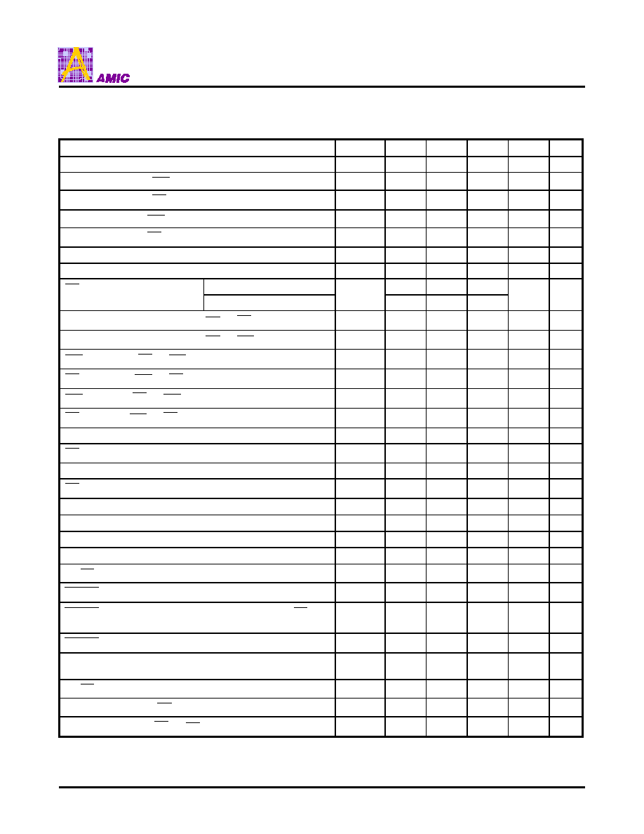
A29DL323 Series
PRELIMINARY (May, 2002, Version 0.0)
31
AMIC Technology, Inc.
AC Characteristics
Write Cycle (Program / Erase)
Parameter
Symbol
Min.
Typ.
Max.
Unit
Notes
Write cycle time
t
WC
85
ns
Address setup time (
WE
to address)
t
AC
0
ns
Address setup time (
CE
to address)
t
AS
0
ns
Address hold time (
WE
to address)
t
AH
45
ns
Address hold time (
CE
to address)
t
AH
45
ns
Input data setup time
t
DS
35
ns
Input data hold time
t
DH
0
ns
Read
0
OE
hold time
Toggle bit, Data polling
t
OEH
10
ns
Read recovery time before write (
OE
to
CE
)
t
GHEL
0
ns
Read recovery time before write (
OE
to
WE
)
t
GHWL
0
ns
WE
setup time (
CE
to
WE
)
t
WS
0
ns
CE
setup time (
WE
to
CE
)
t
CS
0
ns
WE
hold time (
CE
to
WE
)
t
WH
0
ns
CE
hold time (
WE
to
CE
)
t
CH
0
ns
Write pulse width
t
WP
35
ns
CE
pulse width
t
CP
35
ns
Write pulse width high
t
WPH
30
ns
CE
pulse width high
t
CPH
30
ns
Byte programming operation time
t
BPG
9
200
µ
s
Word programming operation time
t
WPG
11
200
µ
s
Sector erase operation time
t
SER
0.7
5
s
1
VCC set time
t
VCS
50
µ
s
RY/
BY
recovery time
t
RB
0
ns
RESET
pulse width
t
RP
500
ns
RESET
high-voltage (V
ID
) hold time from high of RY/
BY
when
sector group is temporarily unprotect
t
RRB
20
µ
s
RESET
hold time
t
RH
50
ns
From completion of automatic program / erase to data output
time
t
EOE
85
ns
RY/
BY
delay time from valid program or erase operation
t
BUSY
90
ns
Address setup time to
OE
low in toggle bit
t
ASO
15
ns
Address hold time to
CE
or
OE
high in toggle bit
t
AHT
0
ns
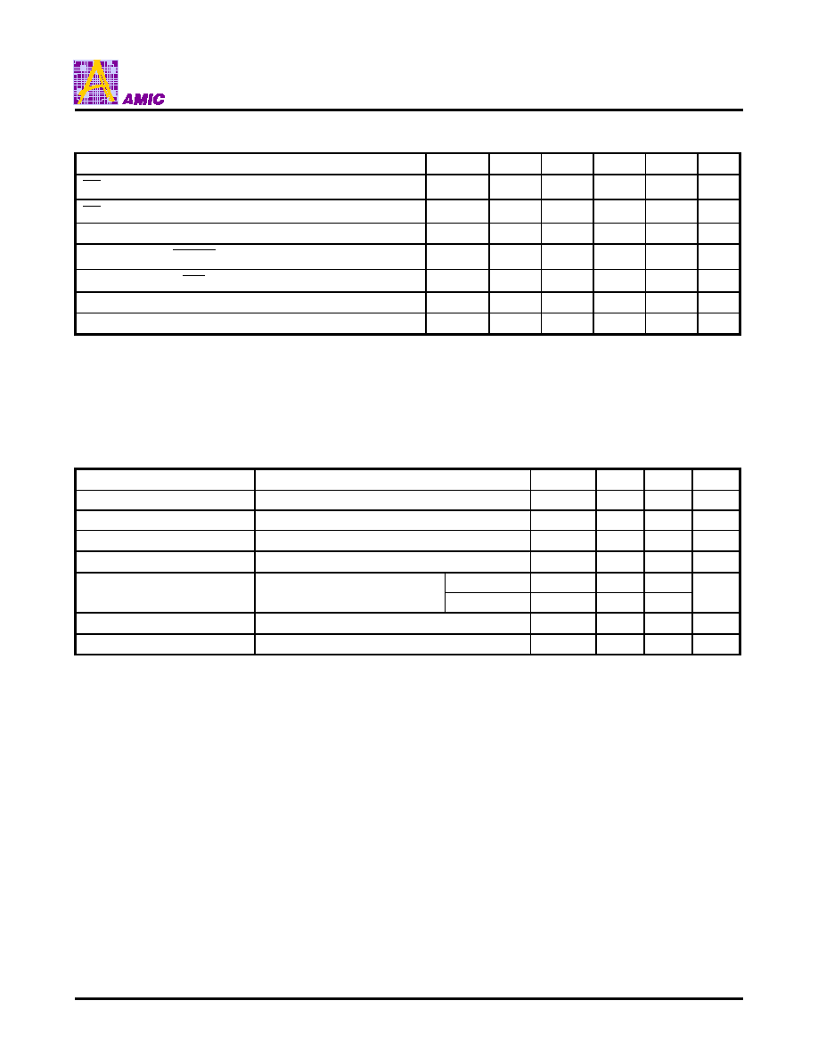
A29DL323 Series
PRELIMINARY (May, 2002, Version 0.0)
32
AMIC Technology, Inc.
Write Cycle (Program / Erase) (continued)
Parameter
Symbol
Min.
Typ.
Max.
Unit
Notes
CE
pulse width high for toggle bit
t
CEPH
20
ns
OE
pulse width high for toggle bit
t
OEPH
20
ns
Voltage transition time
t
VLHT
4
µ
s
2
Rise time to V
ID
(
RESET
)
t
VIDR
500
ns
3
Rise time to V
ACC
(
WE
(ACC))
t
VACCR
500
ns
2
Erase timeout time
t
TOW
50
µ
s
4
Erase suspend transition time
t
SPD
20
µ
s
4
Notes:
1. The preprogramming time prior to the erase operation is not included.
2. Sector group protection and accelerated mode only.
3. Sector group protection only.
4. Table only.
Write operation (Erase / Program) Performance
Parameter
Description
Min.
Typ.
Max.
Unit
Sector erase time
Excludes programming time prior to erasure
0.7
5
s
Chip erase time
Excludes programming time prior to erasure
50
s
Byte programming time
Excludes system-level overhead
9
200
µ
s
Word programming time
Excludes system-level overhead
11
200
µ
s
BYTE mode
40
Chip programming time
Excludes system-level overhead
WORD mode
25
s
Accelerated programming time Excludes system-level overhead
7
150
µ
s
Erase / Program cycle
1,000,000
cycle
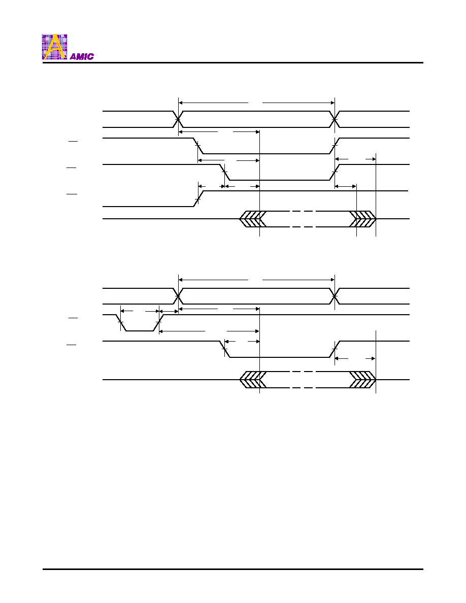
A29DL323 Series
PRELIMINARY (May, 2002, Version 0.0)
33
AMIC Technology, Inc.
Timing Waveform for Read Cycle (1)
Addresses (Input)
Addresses Stable
CE (Input)
OE (Input)
WE (Input)
Data Out
High-Z
I/O (Output)
t
RC
t
OEH
t
OE
t
CE
High-Z
t
OH
t
DF
t
ACC
Timing Waveform for Read Cycle (2)
Addresses (Input)
Addresses Stable
CE (Input)
OE (Input)
Data Out
High-Z
I/O (Output)
t
RC
t
RP
High-Z
t
OH
t
ACC
t
RH
t
READY
t
CE
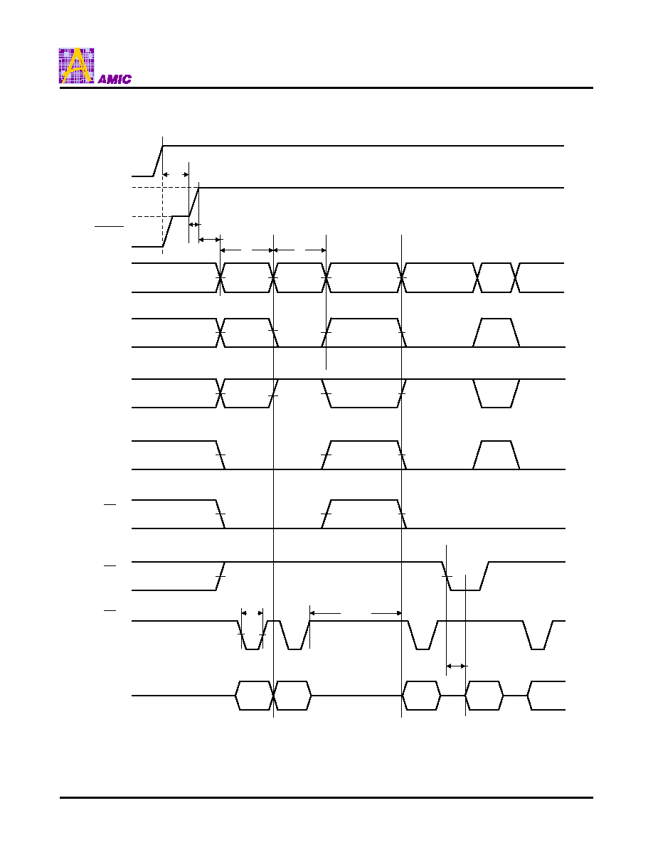
A29DL323 Series
PRELIMINARY (May, 2002, Version 0.0)
34
AMIC Technology, Inc.
Timing Waveform for Sector Group Protection
V
ID
V
IH
RESET
(Input)
Address
(Input)
VCC
t
VCS
t
VIDR
SGAx
SGAx
SGAy
t
OE
t
WP
TIMEOUT
t
WC
t
VLHT
t
WC
A0
(Input)
A1
(Input)
A6
(Input)
CE
(Input)
OE
(Input)
WE
(Input)
I/O
(Input / Outpu)
60H
60H
40H
01H
(Note)
60H
Note: The sector group protection verification result is output
01H: The sector group is protected.
00H: The sector group is not protected
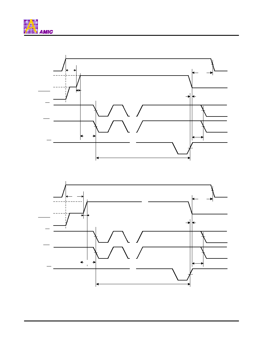
A29DL323 Series
PRELIMINARY (May, 2002, Version 0.0)
35
AMIC Technology, Inc.
Timing Waveform for Temporary Sector Group Unprotect
Program or Erase Command Sequence
~~
~~
t
RRB
WE
(Input)
CE
(Input)
RY/BY
(Output)
~~
V
ID
V
IH
RESET
(Input)
VCC
t
VCS
t
VIDR
t
VLHT
t
VLHT
t
VLHT
Period during which protection is canceled
Timing Waveform for Accelerated Mode
Program or Erase Command Sequence
~~
~~
t
RRB
CE
(Input)
WE
(Input)
RY/BY
(Output)
~~
V
ID
V
IH
RESET
(Input)
VCC
t
VCS
t
VACCR
t
VLHT
t
VLHT
t
VLHT
Accelerated mode period
~~
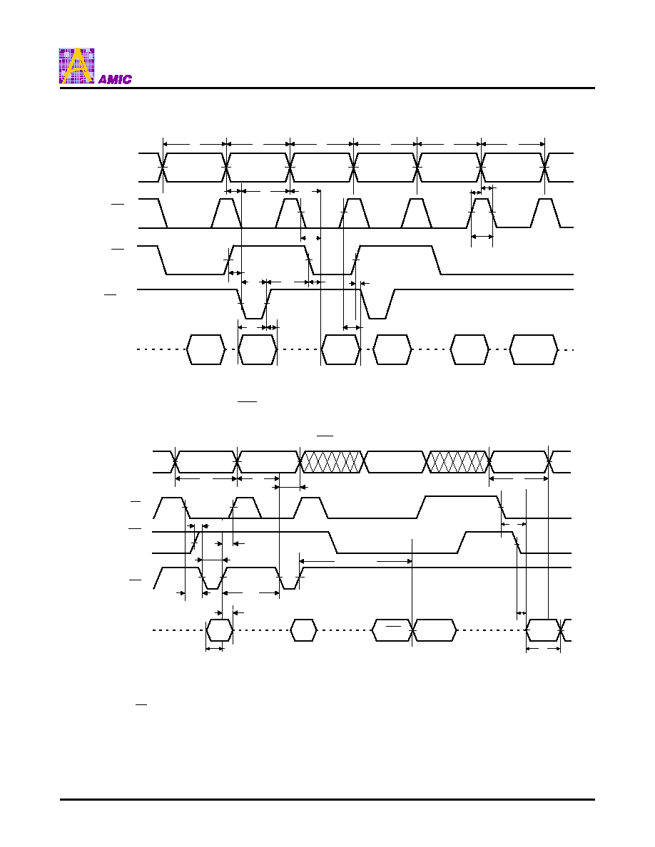
A29DL323 Series
PRELIMINARY (May, 2002, Version 0.0)
36
AMIC Technology, Inc.
Timing Waveform for Dual Operation
Address
(Input)
BA1
Input
BA2
BA1
BA2
BA1
BA2
Output
Input
Output
Status
Output
t
RC
t
WC
t
RC
t
WC
t
RC
t
WC
t
AS
t
AH
t
ACC
t
CEPH
t
AHT
t
AS
t
DF
t
DF
t
CE
t
OE
t
OEH
t
WP
t
GHWL
t
DH
t
DS
CE
(Input)
OE
(Input)
WE
(Input)
I/O
(Input / Outpu)
Timing Waveform for Write Cycle (
WE
Controlled)
Addresses
(Input)
CE
(Input)
OE
(Input)
WE
(Input)
I/O (Input / Output)
555H
PA
D
OUT
I/O
7
Data Polling
Note :
1. This timing waveform shows the last two write cycles among the program command sequence's four write cycles, and data polling.
2. This timing waveform shows the WORD mode's case. In the BYTE mode, address to be input is different from the WORD mode.
See Table 8. Command Sequence.
3. PA : Program address
PD : Program data
I/O
7
: The output of the complement of the data written to the device.
D
OUT
: The output of the data written to the device.
t
BPG
or
t
WPG
t
AS
t
WC
t
WP
t
CS
t
WPH
t
DH
PA
3rd and 4th write cycle
t
AH
t
RC
PD
A0H
D
OUT
t
CE
t
OE
t
OH
t
GHWL
t
CH
t
DS
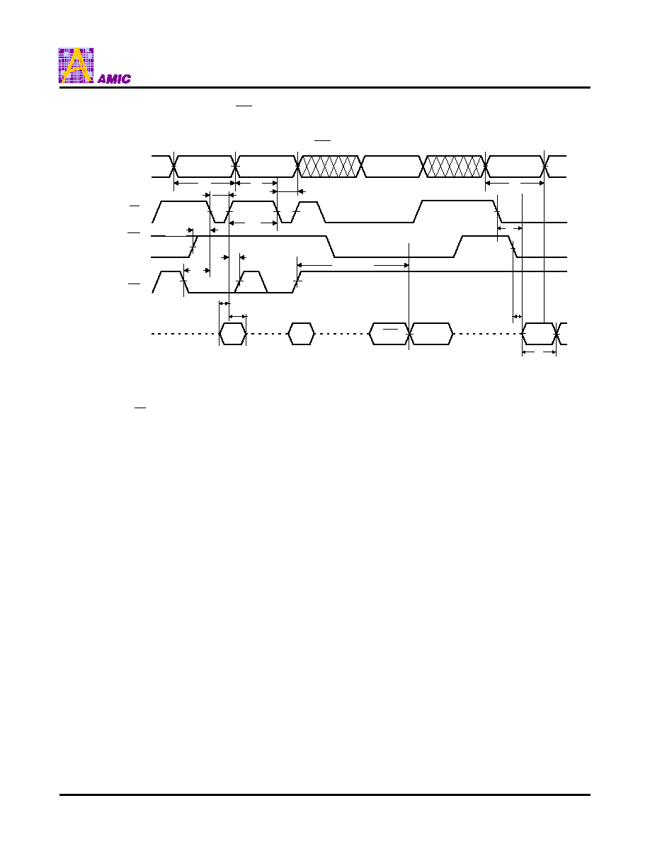
A29DL323 Series
PRELIMINARY (May, 2002, Version 0.0)
37
AMIC Technology, Inc.
Timing Waveform for Write Cycle (
CE
Controlled)
Addresses
(Input)
CE
(Input)
OE
(Input)
WE
(Input)
I/O (Input / Output)
555H
PA
D
OUT
I/O
7
Data Polling
Note :
1. This timing waveform shows the last two write cycles among the program command sequence's four write cycles, and data polling.
2. This timing waveform shows the WORD mode's case. In the BYTE mode, address to be input is different from the WORD mode.
See Table 8. Command Sequence.
3. PA : Program address
PD : Program data
I/O
7
: The output of the complement of the data written to the device.
D
OUT
: The output of the data written to the device.
t
BPG
or
t
WPG
t
AS
t
WC
t
WH
PA
3rd and 4th write cycle
t
AH
t
RC
PD
A0H
D
OUT
t
CE
t
OE
t
OH
t
GHWL
t
DS
t
CP
t
CPH
t
WS
t
DH
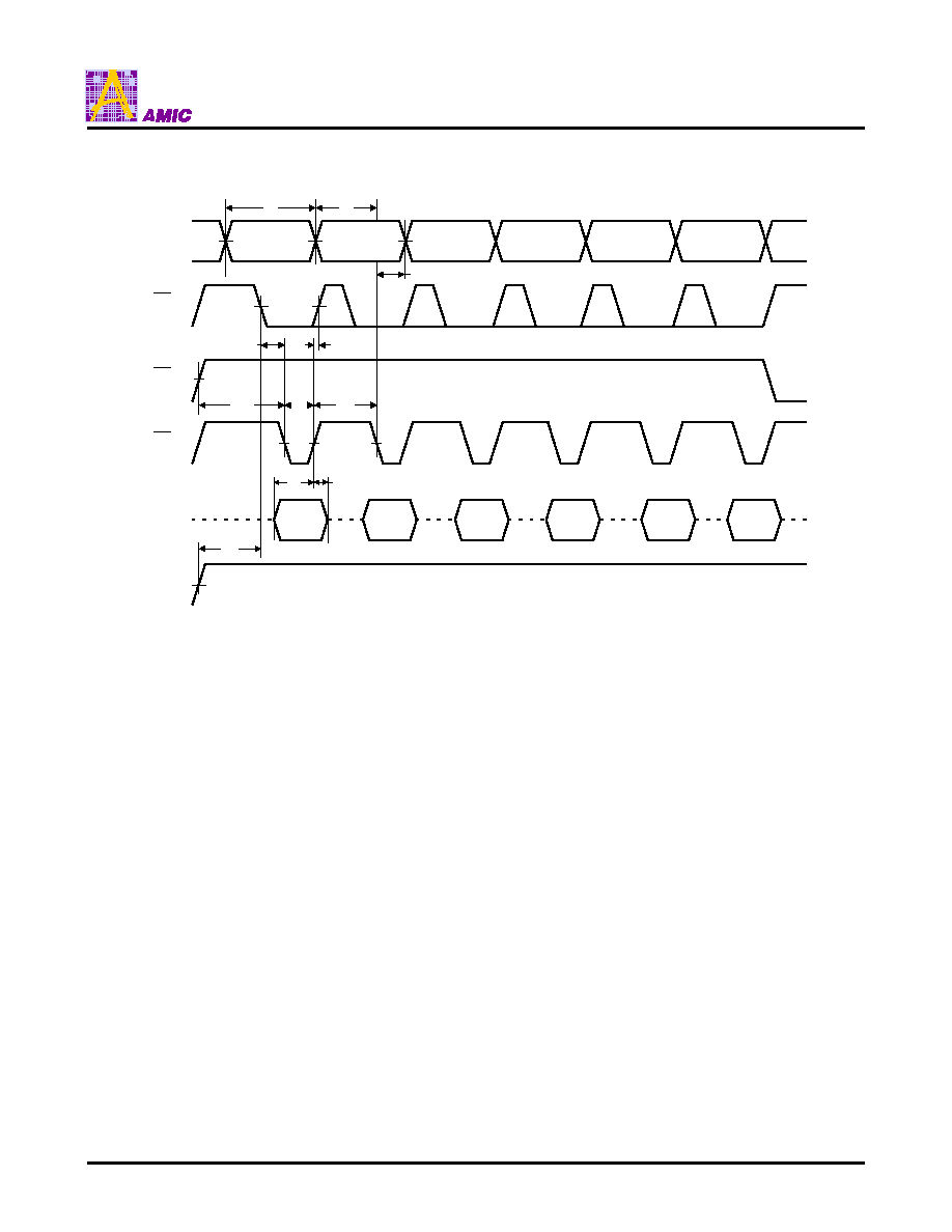
A29DL323 Series
PRELIMINARY (May, 2002, Version 0.0)
38
AMIC Technology, Inc.
Timing Waveform for Sector / Chip Erase
Address
(Input)
555H
55H
2AAH
555H
555H
2AAH
FSA
(Note)
AAH
AAH
80H
55H
t
RC
t
WC
CE
(Input)
I/O
(Input / Outpu)
30H
t
AH
t
CH
t
CS
t
GHWL
t
WP
t
WPH
t
VCS
t
DH
t
DS
(10H for chip erase)
OE
(Input)
WE
(Input)
VCC
Note :
1. FSA is the sector address to be erased. In the case of chip erase, input 555H (WORD mode), AAAH (BYTE mode).
2. This timing chart shows the WORD mode's case. In the BYTE mode, address to be input is different from the WORD mode.
See Table 8. Command Sequence.
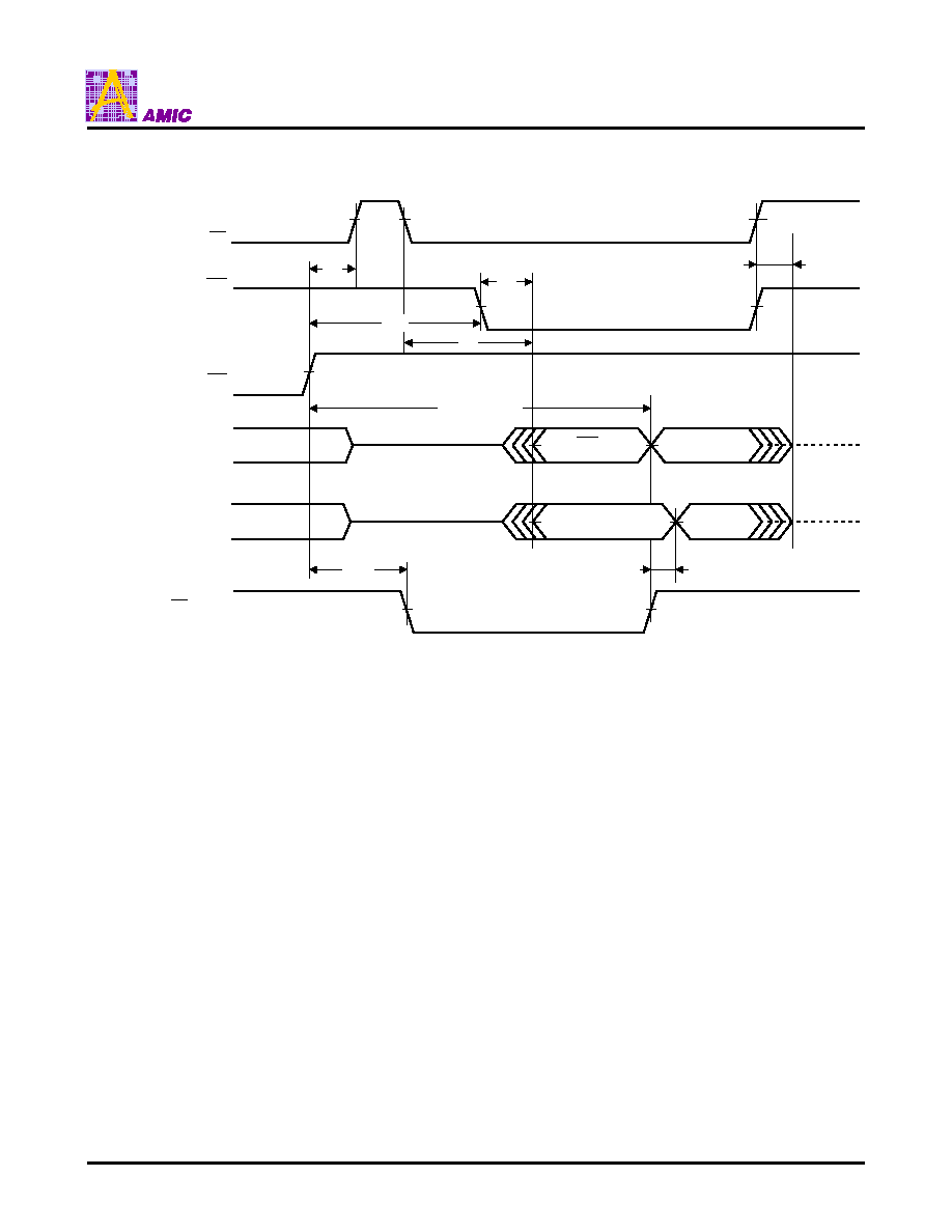
A29DL323 Series
PRELIMINARY (May, 2002, Version 0.0)
39
AMIC Technology, Inc.
Timing Waveform for Data Polling
I/O
7
Status Data
t
DF
Valid Data
D
OUT
(Note)
t
OE
t
CE
t
OEH
t
CH
t
BUSY
t
BPG,
t
WPG,
t
SER
t
EOE
Hi-Z
Hi-Z
CE
(Input)
OE
(Input)
WE
(Input)
I/O
0
-I/O
6
(Output)
RY/BY(Output)
I/O
7
(Output)
Note :
1. I/O
7
= D
OUT
: True value of program data (indicates completion of automatic program / erase)
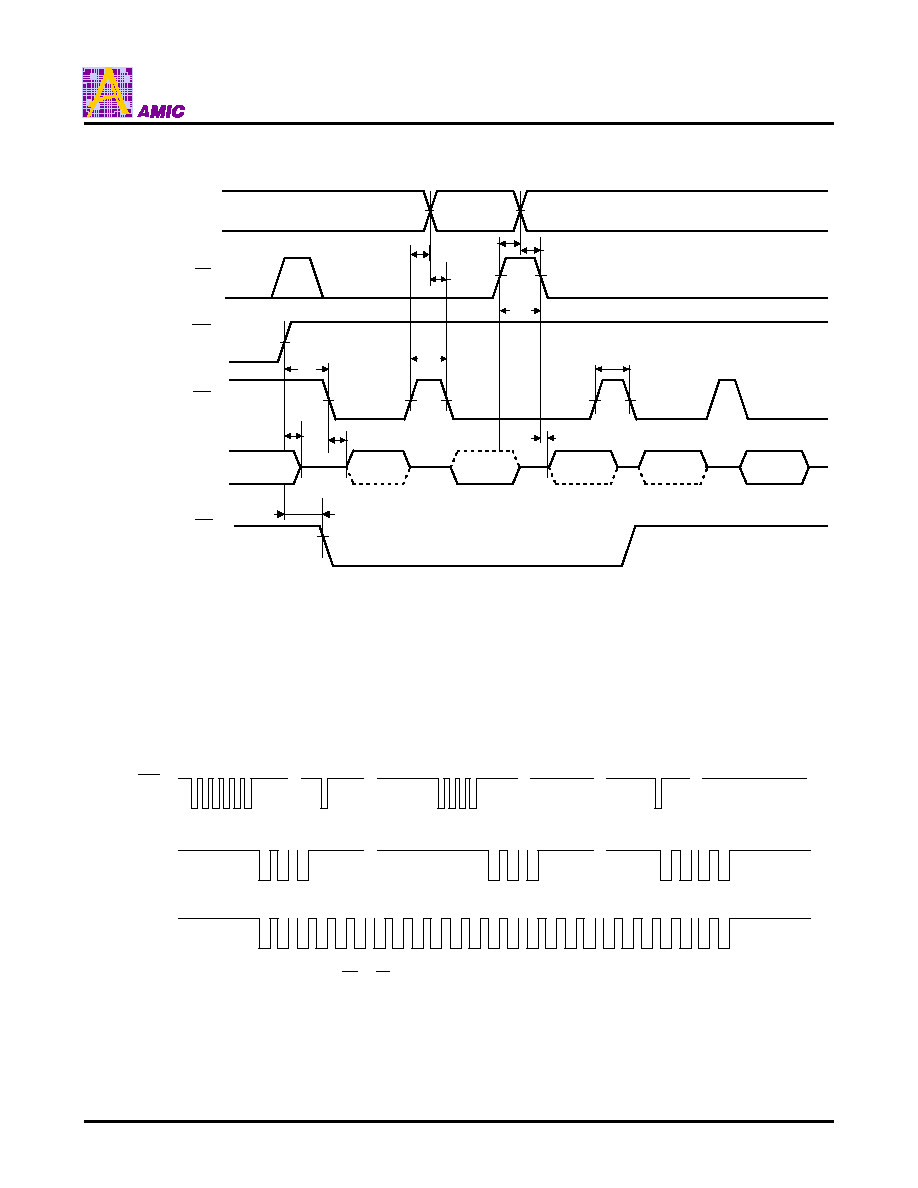
A29DL323 Series
PRELIMINARY (May, 2002, Version 0.0)
40
AMIC Technology, Inc.
Timing Waveform for Toggle Bit
VA
Toggle
Toggle
Toggle
Stop Toggle
(note)
Valid
Data Out
Input Data
t
BUSY
t
OE
t
DH
t
OEH
t
OEPH
t
ASO
t
AHT
t
AS
t
AHT
t
CEPH
t
CE
t
OEH
Addresses
(Input)
CE
(Input)
WE
(Input)
OE
(Input)
I/O
6
, I/O
2
(Input / Output)
RYBY
(Output)
Note :
1. I/O
6
stops the toggle (indicates automatic program / erase completion).
Timing Waveforms for I/O
2
vs. I/O
6
Input of
Automatic Erase
Command
Erase
Suspended
Erase Suspended
Input of Program
Command
Erase
Resumed
WE
(Input)
I/O
6
(Output)
I/O
2
(Output)
Erasure
Erase Suspend
Read
Erase Suspend
Read
Erasure
Completion of
Erasure
Toggle
I/O
2
and I/O
6
(CE or OE is used for toggle)
~ ~
~ ~
~ ~
Erase Suspend Input of
Program Command
~ ~
~ ~
~ ~
~ ~
~ ~
~ ~
~ ~
~ ~
~ ~
~ ~
~ ~
~ ~
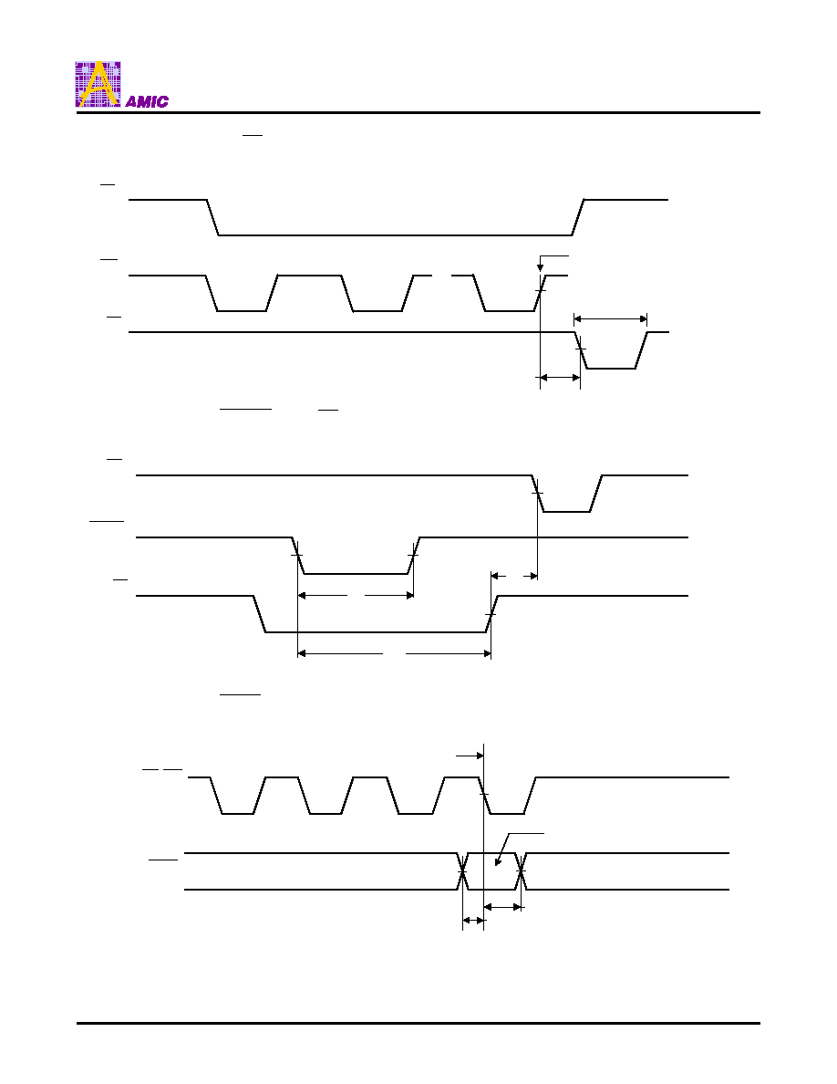
A29DL323 Series
PRELIMINARY (May, 2002, Version 0.0)
41
AMIC Technology, Inc.
Timing Waveform for RY/
BY
(Read / Busy)
~~
t
BUSY
Rising Edge of the Last Write Pulse
Automatic Program or Erase
CE
(Input)
WE
(Input)
RY/BY
(Output)
Timing Waveform for
RESET
/ RY /
BY
t
RPD
t
RB
WE
(Input)
RESET
(Input)
RY/BY
(Output)
t
RP
Timing Waveform for
BYTE
Input Determined
Failing Edge of Last Write Pulse
t
AH
t
AS
OE, WE
(Input)
BYTE
(Input)
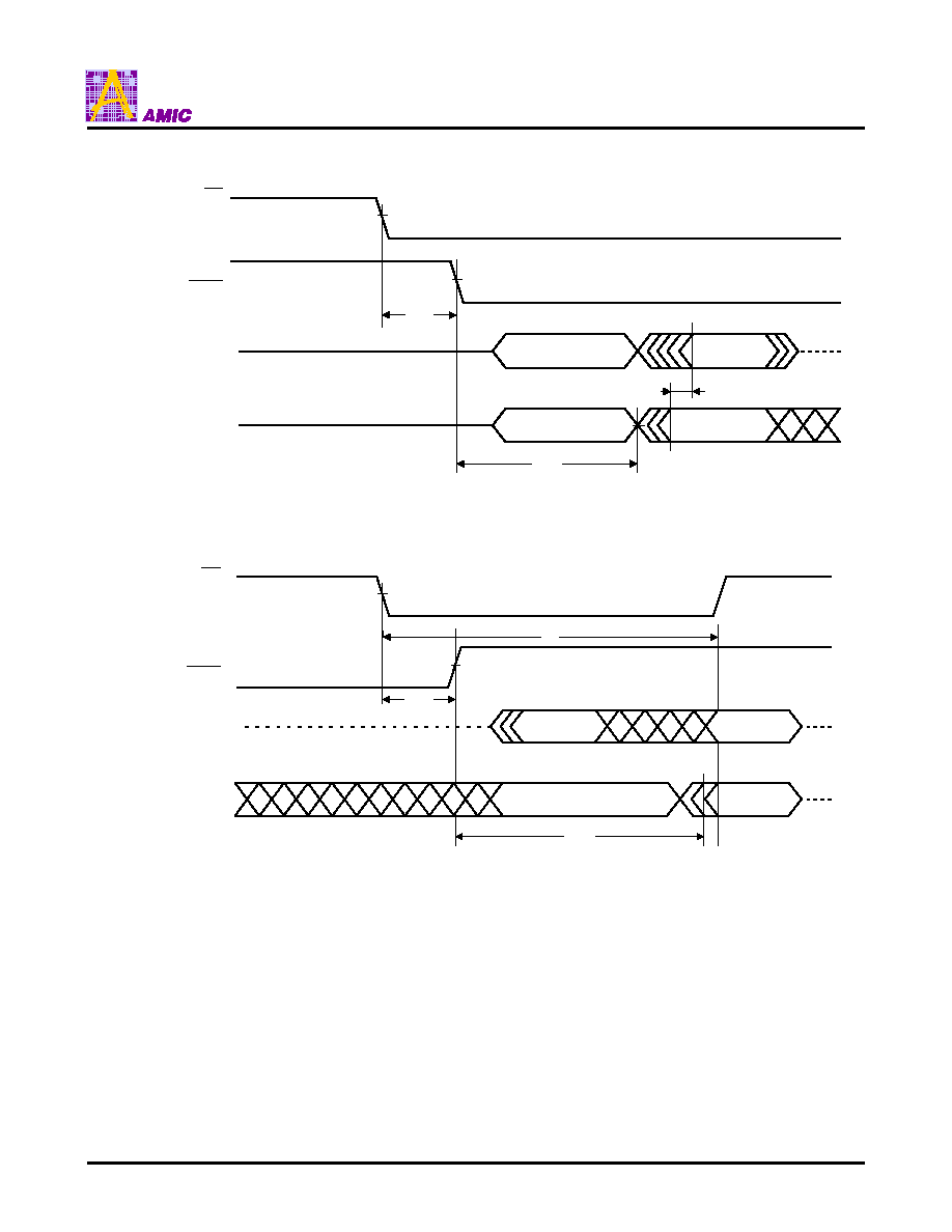
A29DL323 Series
PRELIMINARY (May, 2002, Version 0.0)
42
AMIC Technology, Inc.
Timing Waveform for BYTE Mode Switching
Data Output
I/O
0
to I/O
14
Data Output
I/O
0
to I/O
7
t
ELFL
Hi-Z
CE
(Input)
BYTE
(Input)
I/O
1
5
(Output), A-1(Input)
I/O
0
to I/O
14
(Output)
Data Output
I/O
15
Address Input
A-1
Hi-Z
Hi-Z
t
ACC
t
FLQZ
Timing Waveform for WORD Mode Switching
Data Output
I/O
0
to I/O
7
t
ELFH
Hi-Z
CE
(Input)
BYTE
(Input)
I/O
1
5
(Output), A-1(Input)
I/O
0
to I/O
14
(Output)
Hi-Z
t
FHQV
Data Output
I/O
0
to I/O
14
Data Output
I/O
15
Address Input
A-1
Hi-Z
t
CE
A29DL323 Series
PRELIMINARY (May, 2002, Version 0.0)
43
AMIC Technology, Inc.
Latch-up Characteristics
Description
Min.
Max.
Input Voltage with respect to VSS on all I/O pins
-1.0V
VCC+1.0V
VCC Current
-100 mA
+100 mA
Input voltage with respect to VSS on all pins except I/O pins
(including A9,
OE
and
RESET
)
-1.0V
12.5V
Includes all pins except VCC. Test conditions: VCC = 5.0V, one pin at time.
Capacitance (T
A
= 25
∞
∞
C, f = 1MHz)
Parameter Symbol
Parameter Description
Test Setup
Typ.
Max.
Unit
C
IN
Input Capacitance
V
IN
=0
6
7.5
pF
C
OUT
Output Capacitance
V
OUT
=0
8.5
12
pF
Notes:
1. V
IN
: Input voltage, V
OUT
: Output voltage
2. These parameters are not 100% tested.
Data Retention
Parameter
Test Conditions
Min
Unit
150
∞
C
10
Years
Minimum Pattern Data Retention Time
125
∞
C
20
Years
A29DL323 Series
PRELIMINARY (May, 2002, Version 0.0)
44
AMIC Technology, Inc.
Ordering Information
Part No.
Access Time
(ns)
Operating Supply
Voltage
(V)
Boot Sector
Package
A29DL323TV-90
Top Address (Sector)
(T type)
48Pin TSOP
A29DL323UV-90
Bottom Address (Sector)
(B type)
48Pin TSOP
A29DL323TG-90
Top Address (Sector)
(T type)
63-ball TFBGA
A29DL323UG-90
90
2.7 to 3.6
Bottom Address (Sector)
(B type)
63-ball TFBGA
A29DL323 Series
PRELIMINARY (May, 2002, Version 0.0)
45
AMIC Technology, Inc.
Package Information
TSOP 48L (Type I) Outline Dimensions
unit: inches/mm
1
E
c
D
L
Detail "A"
0.25
24
25
48
D
1
D
y
e
S
A
1
A
2
A
Detail "A"
b
Dimensions in inches
Dimensions in mm
Symbol
Min
Nom
Max
Min
Nom
Max
A
-
-
0.047
-
-
1.20
A
1
0.002
-
0.006
0.05
-
0.15
A
2
0.037
0.039
0.042
0.94
1.00
1.06
b
0.007
0.009
0.011
0.18
0.22
0.27
c
0.004
-
0.008
0.12
-
0.20
D
0.779
0.787
0.795
19.80
20.00
20.20
D
1
0.720
0.724
0.728
18.30
18.40
18.50
E
-
0.472
0.476
-
12.00
12.10
e
0.020 BASIC
0.50 BASIC
L
0.016
0.020
0.024
0.40
0.50
0.60
S
0.011 Typ.
0.28 Typ.
y
-
-
0.004
-
-
0.10
0∞
-
8∞
0∞
-
8∞
Notes:
1. The maximum value of dimension D includes end flash.
2. Dimension E does not include resin fins.
3. Dimension S includes end flash.
A29DL323 Series
PRELIMINARY (May, 2002, Version 0.0)
46
AMIC Technology, Inc.
Package Information
63 BALLS
TFBGA
(7 x 11mm) Outline Dimensions
unit: mm
0.05
11.00
±
8 7 6 5 4 3 2 1
A
B
C
D
E
F
G
H
J
K
L
M
4
5.6
0.7
8.8
0.8
1.1
7.00
0.05
±
Ball#A1 CORNER
A
0.10
C
M
0.05
M
B C
0.35
A
B
Ball*A1 CORNER
TOP VIEW
BOTTOM VIEW
SIDE VIEW
C
SEATING PLANE
//
0.1
C
1.2 MAX.
0.05
0.25
±
0.08 C